/
Zynq-7000 AP SoC - Zynq BFM Simulation of Packet Processing Unit in PL Tech Tip
Zynq-7000 AP SoC - Zynq BFM Simulation of Packet Processing Unit in PL Tech Tip
- Confluence Wiki Admin (Unlicensed)
Owned by Confluence Wiki Admin (Unlicensed)
Sept 24, 2018
Zynq-7000 AP SoC - Zynq BFM Simulation of Packet Processing Unit in PL Tech Tip
Document History
| Date |
Version |
Author |
Description of Revisions |
| 11/12/2013 |
0.1 |
E. Srikanth |
Initial Draft |
Introduction
The following tech-tip describes on how to use Zynq SoC Bus Functional Model (BFM) to perform functional simulation of Zynq-7000 based applications. The Zynq BFM is targeted to enable the functional verification of Programmable Logic (PL) by mimicking the PS-PL interfaces and OCM/DDR memories of Processor System (PS) logic.The Zynq BFM is used to replace the whole of the processing system for the purpose of accelerating the simulation. The principle is simple—what code the processor runs does not matter; the peripheral is only concerned with transactions from the processing system to itself. Simulating a full processing system (and the software that it is running) is a very time-consuming process. Removing all unnecessary gates and modules will greatly speed up the simulation, allowing the designer to verify what is needed in the shortest amount of "wall time". Multiple peripherals can be simulated simultaneously.
The BFM produces a user-specified set of bus transactions that mimic the bus behavior of the processing system. A BFM facilitates simulating and verifying the functionality of an IP core quickly without a complete system having to be built. A BFM generates bus transactions for a device under test (DUT) by utilizing a BFM-modeled processor to write bus transactions using API tasks in a Verilog-based test bench. You can add other peripheral cores that connect to the AXI interconnect and include their operation in the simulation model.
The tech-tip is based on the reference design used for Redirecting Ethernet Header to Cache via PL and ACP port Tech tip. In this tech-tip the Ethernet data received by the Gigabit Ethernet Interface on the Zynq PS is redirected to PL for packet inspection and moved to L2 Cache via the ACP port.
The design files for the this tech tip can be downloaded from the following link : Zynq7000AP_SoC_ZynqBFMSimPacketProcessingUnit_design.zip
System Requirements for running the design:
- OS : Windows , Linux
- RAM : 10 GB or greater
- Hard Disk : 40 GB or greater
Zynq BFM Description
The Zynq-7000 BFM is intended to provide a simulation environment for the Zynq-7000 PS logic. Starting Vivado v2013.3, the processing_system7 block in the block design is replaced with its equivalent Bus Functional Model enabling the user to perform verification of the PL Logic connected to the processing_system7. The Zynq-7000 BFM models the following:
- Transactions originating from PS masters through the AXI BFM master API calls
- Transactions terminating through the PS slaves to models of the OCM and DDR memories through interconnect models
- FCLK reset and clocking support
- Input interrupts to the PS from PL
- PS register map
Zynq-7000 BFM consists of four main layers. Figure 1 show the Zynq-7000 BFM architecture.
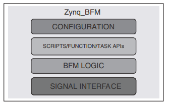 |
| Figure 1: Zynq-7000 BFM Architecture |
- Configuration: Configuration is implemented using Verilog parameters and is used to configure the Zynq-7000 BFM. Some configuration must be done using configuration APIs.
- Function and Task APIs: Verilog tasks and functions that help to set:
- Data path between processing system (PS) and programmable logic (PL) in memory mapped interfaces.
- Control path between PS and PL in register interface.
- Configure the traffic profiles for each ports.
- BFM Logic: BFM logic has the PS-PL interface with supporting functionality that contains the AXI interfaces, sparse memory implementation, and the interconnect (arbiter) model as shown in Figure 2.
- Signal Interface: The signal interface includes the typical Verilog input and output ports and associated signals.
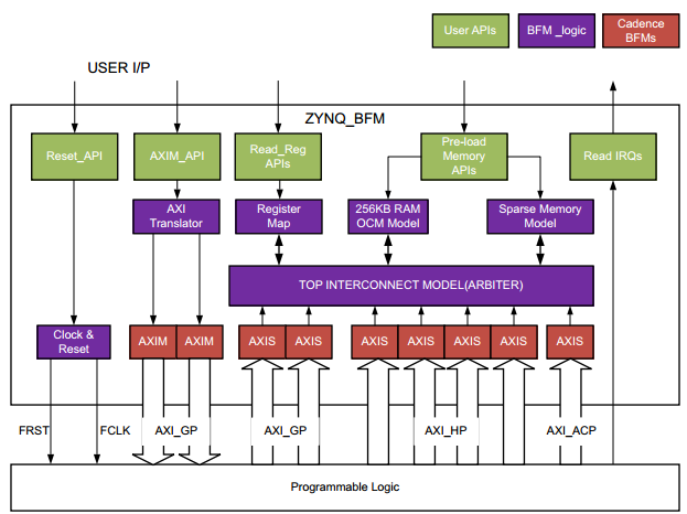 |
| Figure 2: Architecture Details |
The configuration parameters and the APIs necessary for using the Zynq-7000 BFM is described in details in the Zynq-7000 SoC Bus Functional Model Data Sheet(DS897).
Note on limitations of the Zynq BFM: The Zynq BFM cannot emulate any peripheral interrupts that are visible to the Zynq PL. Any PL logic that is using the PS peripheral Interrupts will not have any effect with the Zynq BFM. Instead this peripheral interrupt from PS can be made external and be forced to required value in the testbench as shown in this tech tip.
Design Details:
As in any Zynq-7000 Processing System based block design, the processing_system7 block is instantiated in a common top file along with any desired PL logic with all necessary connections between the PL logic and the processing_system7 block. The processing_system7 block in the block design is replaced with its equivalent Bus Functional Model enabling the user to perform verification of the PL Logic connected to the processing_system7.The design used in this tech-tip basically comprises of a PL logic called Ethernet Packet Processing Unit.
The Ethernet Packet Processor Unit is a custom IP which redirects Ethernet data received on the General Purpose Master AXI port 1 (MAXI GP1) port to the Accelerator Coherency Port (ACP) or the High Performance(HP) port of the Zynq Processing system.
The Ethernet Packet Processing Unit has two AXI-4 slave interfaces as described below.
- Control Port: This AXI-4 Slave interface provides access to all the control and status registers of the Packet Processing Unit. This port is connected to the MAXI GP0 port of the Zynq PS.
- Data Port: This AXI-4 Slave interface provides a data path through which redirected Ethernet packet from Zynq PS is stored into the in-built FIFOs connected behind this interface.
The Ethernet Packet Processing Unit has two AXI4 Master interfaces as described below.
- AXI-4 Master Header Port which is connected to the ACP interface via the AXI-Interconnect.
- AXI-4 Master Payload port which connected to the HP0 interface via the AXI-Interconnect.
There are additional two interrupt pins described as follows.
- interrupt_in: It is input pin connected to the PS Ethernet Interrupt pin which indicates that PS Ethernet Controller has successfully placed the packets in its destination.
- interrupt_out : It is an output pin connected to the PL-PS GIC input (Global Interrupt Controller) of the Zynq PS. The interrupt indicates that Packet Processing unit has successfully placed the packet in the PS memory.
The Ethernet Packet Processor IP allow only the Ethernet Headers to be pushed into the Caches via the ACP port and the rest of the pay load is pushed to the DDR3 memory directly via the HP port. This was done to make sure that the Processor gets the Ethernet Headers readily available for processing without invalidating or flushing the cache.
Brief Block diagram of the Ethernet Packet Processor IP that is implemented in PL is as shown below.
 |
| Figure 3: Inside the Ethernet Packet Processing Uni |
The information regarding the Ethernet Packet Processing Unit is explained in the Redirecting Ethernet Header to Cache via PL and ACP port Tech tip.
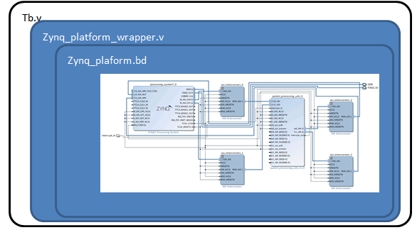
The Block Design for the interconnections between Zynq Processing System and the Ethernet Packet Processing Unit using the Vivado IPI for the Zynq Processing system is as shown below.
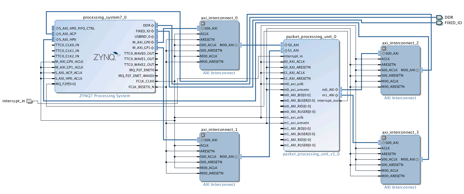
Figure 4: Interconnection between the Zynq PS7 and the PL Logic
Testbench hierarchy
The following hierarchy has been followed to apply stimulus that is present in the tb.v file.
 |
| Figure 5: Testbench Hierarchy |
To access any of the BFM API’s the total hierarchy of the processing_system7 instance should be specified in the test bench file.
For example: In order to use the write_data API of the Zynq BFM specify the complete hierarchy followed by .inst tag
zynq_sys.zynq_platform_i.processing_system7_0.inst.write_data (addr, size, data, response);
Description of the tb.v file:
The tb.v file instantiates the Zynq Platform Block design and the required stimulus to generate the clock and the reset for the Zynq Processing system. Note that applying external reset to processing_system7 will not reset the PL logic. The reset to the PL logic is only asserted by writing to the FPGA_RST_CTRL register which is achieved by the “fpga_soft_reset” API and can be seen in the tb.v file provided with the design.
The tb.v file has the required stimulus to create an arbitrary IPv4, ARP and legacy 802.3 Ethernet Packet format and applying it to the packet processing logic in the PL. The tb.v file does an initial configuration of the packet processing unit via the Control Port which is an AXI4 Slave interface connected to the General Purpose Master AXI port 0 (MAXI_GP0) of the processing_system7.
The initial configuration of the packet processing unit includes operation like programming the “RX Buffer Address Size” register for the number of Buffer descriptors to be used, program the “RX Buffer Address” registers with the Memory Destination Addresses and program the Control Register of the Packet processing unit to run the Packet Processing Operation. The Packet processing IP can support Buffer addresses up to 256.
The entire configuration is performed using write_data API of the Zynq BFM.
Note: Any “write_data” API generates an AXI write transaction on the GP master port that is less than or equal to 128 bytes. The write data is a blocking task and will return only after the AXI write is completed via a write response (BRESP).
After the Packet processing logic is initialized, the Ethernet Packets are prepared and transmitted via the General Purpose Master AXI port 1 (MAXI GP1). The Zynq BFM is capable of redirecting the data either via the MAXI GP0 port or MAXI GP1 port depending on the Address provided for the write_data API.
In case of generating burst transaction write_data_burst API has been used to generate the Ethernet Burst transactions. Currently the Zynq BFM does not provide an API to read the OCM or DDR3 Memory but the Ethernet Transactions can be observed on the AXI bus interfaces of the Packet processing unit.
Implementation
| Implementation Details |
|
| Design Type |
PL |
| SW Type |
- |
| CPUs |
1 ARM Cortex-A9 666MHZ |
| PS Features |
|
| PL Features |
Custom IP(Ethernet Packet Processing Unit ) |
| Boards/Tools |
ZC702 (Ideally No board required) |
| Xilinx Tools Version |
Vivado 2013.3 |
| Files Provided |
|
| Zynq7000AP_SoC_ ZynqBFMSimulationofPacketProcessingUnitinPL_design.zip |
See Appendix A for the descriptions of the files |
Step by Step Instructions
- Copy the Zynq7000AP_SoC_ ZynqBFMSimulationofPacketProcessingUnitinPL_design.zip file to your hard drive and unzip the file to C drive.
- Open the Vivado IDE 2013.3 tool
- Select Open Project à Browse Project to open an existing project.
- Browse to the "C:\Zynq7000AP_SoC_ZynqBFMSimulationofPacketProcessingUnitinPL_design\zynq_bfm_sim\design” folder where the Vivado project is present.
- Select the zynq_bfm_sim.xpr file and Select OK.
- The Vivado tool should show the project open.
- In the Source View under Design Sources, expand the zynq_platform_wrapper.v file.
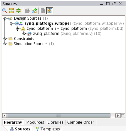
Figure 6: Design Hierarchy - Double click on the zynq_plaform.bd file to open the Zynq Block design. Check the inter-connections between the processing system and the packet processing unit as shown below.

Figure 7: Zynq_platform Block Design. - Switch to the Source view again and under Simulation Sources, expand the sim1 folder to see the hierarchy under the simulation sources
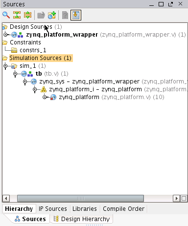
Figure 8: Simulation Sources
You can see that there is a top level test bench file which has instantiated the zynq_platform_wrapper file. This is similar to the simulation hierarchy as explained in the test bench hierarchy section. - Double click the tb.v file under simulation sources to view the file in the Vivado text editor.
- Carefully observe the tb.v file and you would see that the Zynq BFM APIs are used to generate the AXI single beat and burst transactions for the PL Logic configuration and bus transactions.
- Ensure that the tb.v file is selected as the top module under Simulation sources, click on the Run Simulationà Run Behavioral Simulation Button.

Figure 9: Running the Behavioral Simulation
The Vivado tool starts the compilation and elaboration process of the design and the test bench and then and opens the simulation view and opens the wave form viewer. - By default the waveform viewer displays the only the signals present in the tb.v file. To see the signals of our interest an existing waveform configuration zynq_bfm_sim.wcfg has already been provided with the design files and is present in the “\zynq_bfm_sim\sim” directory
- Select File-> Open Waveform configuration and browse to “\zynq_bfm_sim\sim” directory and select the zynq_bfm_sim.wcfg file to open a new waveform window.
- Select Runà Restart to restart the simulation.
- Select Runà Run All to run the simulation till the end.
Observations
In the zynq_bfm_sim.wcfg file AXI Interface signals and registers of the Packet Processing Unit have been organized as follows.- Under PPU_SLAVE_0 divider we see all the signals and transactions that the Zynq BFM is writing to the Packet Processing Unit AXI slave port 0.
- Under PPU_SLAVE_1 divider we see all the transactions of the signals that the Zynq BFM is writing to the Packet Processing Unit AXI slave port 1 which is actually the emulated Ethernet traffic on MAXI_GP1 port.
- Under PPU_ACP divider we see all the transactions of the signals that the Packet Processing Unit Master Port is writing to the ACP port of the Zynq BFM. This is the Header data that is being redirected to the ACP port for Header inspection by the processor.
- Under PPU_HP0 divider we see all the transactions of the signals that the Packet Processing Unit Master Port is writing to the High Performance port of the Zynq BFM. This is the Ethernet payload data that is being redirected to the DDR.
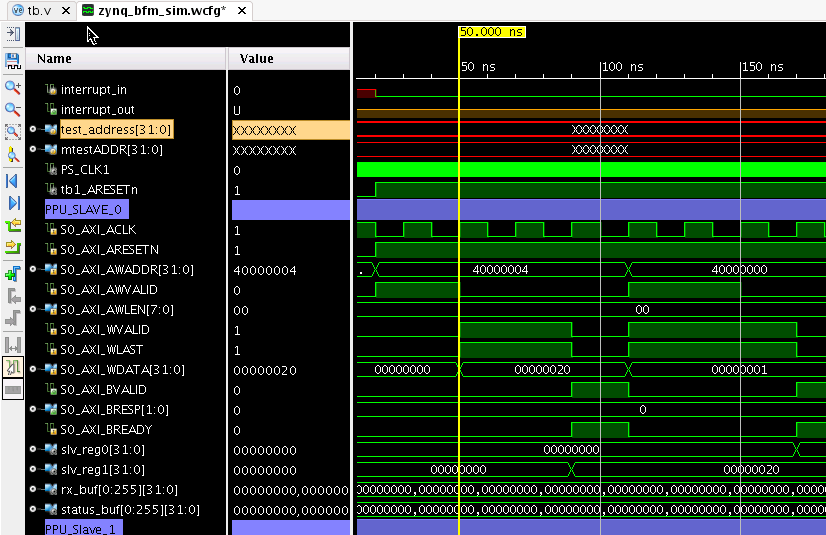
Figure 10: Packet Processing Unit Slave port 0 Signals and Registers.
- At approximately 50 ns as shown above, you will see that the packet processing unit has been configured with the number of BDs to be used which is approximately equal to 32 ( 0x20). This AXI transaction was generated by the write_data API present in the tb.v file at line number 248.
- Then at approximately 110 ns you will see that the Packet processing unit has configured to start the packet processing engine by writing 0x1 to the Control register (slv_reg0) This AXI transaction was generated using the write_data API present in the tb.v file at line number 256.
- From 170 ns to 3000 ns as shown below the Address Buffer register have been programmed with the memory addresses the packet processing unit has to redirect the packet to the memory. This AXI transactions were again generated using the write_data API using a for statement in the tb.v file between line numbers 267 to 273.

Figure 11: Packet Processing Unit configured with addresses of the Zynq Memory. - From 3000 ns under PPU_SLAVE_1 divider you will see the Ethernet traffic being redirected to the AXI Slave Port 1 of the Packet processing unit as shown below. These transactions have been generated using the write_burst API present in the logic implemented between the line numbers 304 to 467.
The logic generates five packets of IPv4 , ARP and Legacy Ethernet packet types to packet processing logic. The number of packets can be changed by modifying the loop count . Similarly the packet type can be changed by modifying the test_data[0] type field in the test bench.
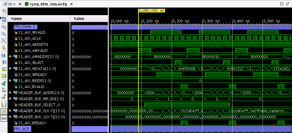
Figure 12: Packet Processing Unit Slave Port 1 Signals - From 3.4 us under PPU_ACP divider and PPU_HP0 you will see how the header information redirected to the ACP port and payload information is redirected to the DDR via the HP0 port for different packet types.
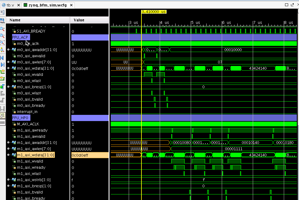
Figure 13: Packet Processing Unit Master Port 0 and Master Port 1 signals
4. Conclusion
This techtip demonstrates how the Packet Processing unit logic can be functionally simulated using Zynq BFM. This tech tip also guides you through conducting a Bus Functional Model (BFM) simulation of PL logic using Zynq BFM for Zynq-7000 based applications. Zynq BFM is used to replace the whole of the processing sys for the purpose of accelerating the simulation., multiple selections available,
Related content
Zynq-7000 AP SoC - Performance - Ethernet Packet Inspection - Linux - Redirecting Packets to PL and Cache Tech Tip
Zynq-7000 AP SoC - Performance - Ethernet Packet Inspection - Linux - Redirecting Packets to PL and Cache Tech Tip
More like this
Zynq-7000 AP SoC - Performance - Ethernet Packet Inspection - Bare Metal - Redirecting Packets to PL Tech Tip
Zynq-7000 AP SoC - Performance - Ethernet Packet Inspection - Bare Metal - Redirecting Packets to PL Tech Tip
More like this
Zynq-7000 AP SoC - Performance - Ethernet Packet Inspection - Bare Metal - Redirecting Headers to PL and Cache Tech Tip
Zynq-7000 AP SoC - Performance - Ethernet Packet Inspection - Bare Metal - Redirecting Headers to PL and Cache Tech Tip
More like this
Zynq-7000 AP SoC - Implementing a Host PC GUI for Communication with Zynq Tech Tip
Zynq-7000 AP SoC - Implementing a Host PC GUI for Communication with Zynq Tech Tip
Read with this
Zynq-7000 AP SoC - Read and Write to the Zynq OCM from The PL
Zynq-7000 AP SoC - Read and Write to the Zynq OCM from The PL
Read with this
Zynq-7000 AP SoC Performance & Benchmarks
Zynq-7000 AP SoC Performance & Benchmarks
More like this
© Copyright 2019 - 2022 Xilinx Inc. Privacy Policy