Zynq-7000 AP SoC - Read and Write to the Zynq OCM from The PL
Zynq-7000 AP SoC - Read and Write to the Zynq OCM from The PL
Table of Contents
Introduction
This article shows how to create an IP with a master full AXI4 interface used to read and write from the Programmable Logic (PL) to the On-Chip Memory (OCM) of the Processing System (PS) using the zynq S_AXI_HP0 slave interface. It uses Vivado/SDK 2017.1 and targets a ZC702 board.Step 1 : Create a new Vivado 2017.1 project
Open Vivado 2017.1 and create a new project targeting the Xilinx ZC702 boardStep 2 : Create an new IP with a master full AXI4 interface
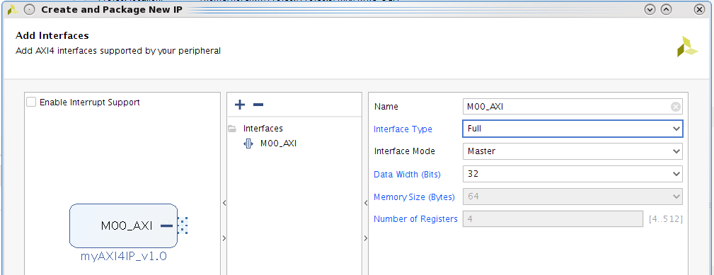
In Vivado 2017.1, click on Tools > Create and Package New IP. Create a nex AXI4 peripheral called myAXI4IP.On the Add Interfaces page, add a new 32-bit master full AXI4 Interface
Then package the IP without editing it.
Vivado as generated a template for the IP. The IP will write data to the SLAVE_BASE_ADDRESS (entered when configuring the IP) and then read the data back to check that the write was successful. The data written should be 0x1,0x2...0xn to the addresses SLAVE_BASE_ADDRESS, SLAVE_BASE_ADDRESS + 0x4 ... SLAVE_BASE_ADDRESS 0x4*n (with n the burst length entered when configuring the IP).
We could check validate the functionality of the IP in simulation with the AXI VIP (this is shown in this wiki page)
Step 3 : Create the Vivado design
As per the UG585:"The four AXI_HP interfaces (from the PS) provide PL bus masters with high bandwidth datapaths to the DDR and OCM memories."
So in this part we will connect the newly created IP to the zynq S_AXI_HP0 slave interface
In the main project, create a new Block Design (BD) and add a Zynq-7.
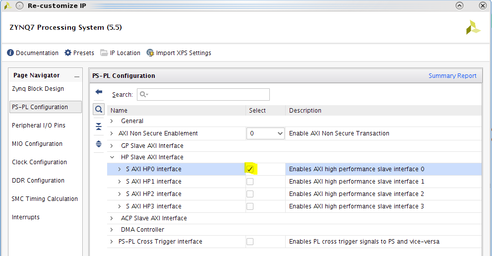
In the Zynq-7 GUI, load the preset configuration for the ZC702 board. Then in the PS-PL configuration page, enable the S_AXI_HP0 slave interface:
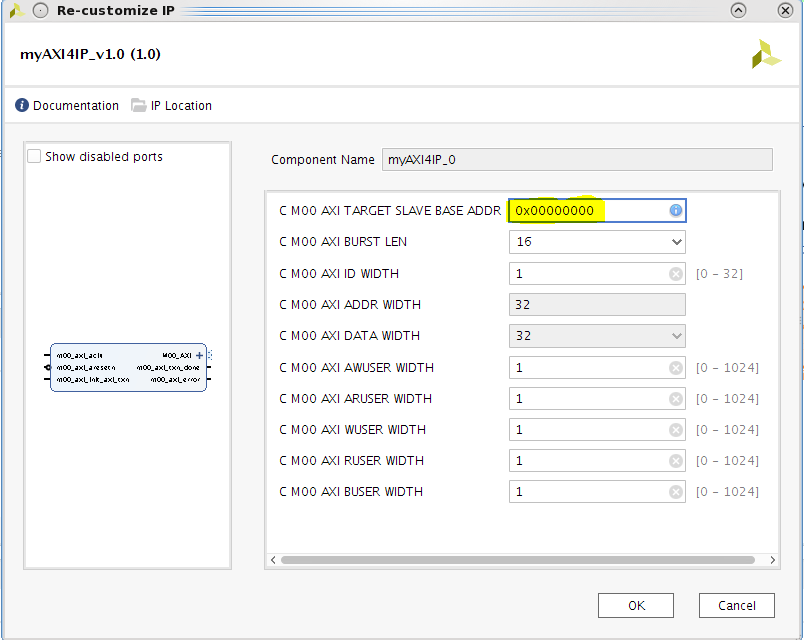
Add the IP myAXI4IP to the BD and configure the IP to target a slave with the base address 0x00000000 (which is the address of the OCM):
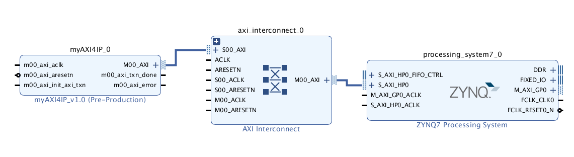
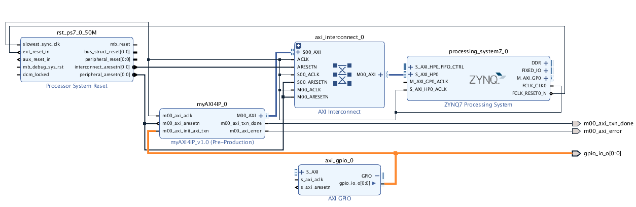
The S_AXI_HP0 slave interface of the Zynq-7 is an AXI3 interface while our IP has an AXI4 interface. Thus, we need an AXI interconnect IP to do the bridge between the 2 interfaces. Add the
AXI interconnect IP and connect the M_00_AXI master (myAXI4IP) and S_AXI_HP0 slave (zynq) interfaces to it.
Click on “Run Connection Automation” to let Vivado do all the other connections. Set the ports m00_axi_txn_done and m00_axi_error of the myAXI4IP_0 as external port (right-click on the ports > make external).
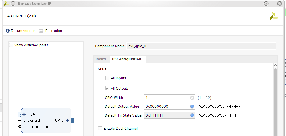
The IP we have created in step 1 needs a pulse to start writing to the OCM. We will generate this pulse in SW and an AXI GPIO IP. Add an AXI GPIO IP with the following configuration:
Make the GPIO output pin as external and connect it also to m00_axi_init_axi_txn of myAXI4IP:
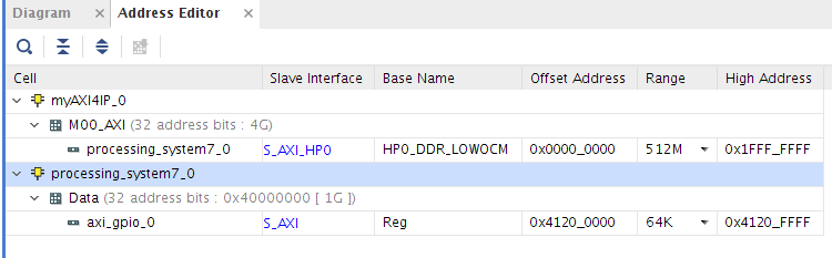
In the address Editor page, click on “Auto Assign Addresses”. We can see that this assign the addresses 0x0000_0000 for the OCM and 0x4120_0000 for the AXI GPIO IP
Validate the design, create the HDL wrapper and generate the BD output products.
Add the following constraint file to the project:
Run synthesis/Implementation and generate the bitstream. Then export the hardware to SDK including the bitstream and launch SDK.
Step 4 : Test the design in Xilinx SDK
In SDK, create a new application project with the Hello World template.Start debugging the application using the system debugger, then program the FPGA.
In the XSCT console, write data to the base address of the OCM using the following commands:
xsct% target 3
xsct% mwr 0x0 0x12345678
xsct% mwr 0x4 0xabcd1234
We can check that the values are correctly written:
xsct% mrd 0x0
0: 12345678
xsct% mrd 0x4
4: ABCD1234
Then in the XSCT console enter the following commands to enable the myAXI4IP IP to write to the OCM:
xsct% mwr 0x41200000 0x1
xsct% mwr 0x41200000 0x0
We can check that data have been written by reading back to the OCM:
xsct% mrd 0x0
0: 00000001
xsct% mrd 0x4
4: 00000002

The myAXI4IP IP also check that the data are correctly written by reading them back. We can see on the ZC702 board that the LED DS20 is off, signalling no error in the write.
Related Links
Do more:© Copyright 2019 - 2022 Xilinx Inc. Privacy Policy