Zynq-7000 AP SOC Secondary Boot Over PCIe Techtip
Zynq-7000 AP SOC Secondary Boot Over PCIe Techtip
Table of Contents
Document History
| Date |
Version |
Author |
Description of Revisions |
| 4/2/2015 |
1.0 |
Bokka Abhiram Saikrishna Anil Kumar A V Mrinal J Sarmah |
Initial release |
Description/Summary
The focus of this application note/Tech tip is on implementation of a Secondary boot mechanism for the Zynq-7000 System on Chip (SoC). Initially BootROM and first stage boot loader (FSBL) are executed, and then u-boot. Loading u-boot from an external source like SD over QSPI is the primary boot mechanism. This application note describes the implementation of secondary boot mechanism where the u-boot image will be transferred from an external host machine over PCI Express link to Processing System DDR memory.
Introduction
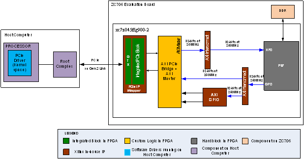
The Zynq-7000 SoC integrates a dual core ARM® Cortex™-A9 MPCore™ based PS and PL in a single device.The PL includes the programmable logic, configuration logic, and associated embedded devices. The PS comprises the processor unit, on-chip memory, external memory interfaces, and peripheral connectivity interfaces including two gigabit ethernet controllers (GEM), which access PL signals through the extended multiplexed I/O (EMIO) interface to connect different physical interfaces. The focus of this application note is to implement software and hardware design on the Zynq-7000 SoC that makes possible the retrieval of a secondary boot image from an external host system over PCI Express. Secondary boot option allows the user to load desired application to be executed by Zynq, after the system initialization is done by the First Stage Boot Loader (FSBL). Hence, it eliminates the need to flash the application (secondary boot image) along with FSBL. Figure 1 shows the functional block diagram of the implementation and data flow from host computer to the PS DDR memory. The secondary boot image (u-boot in the current implementation) resides in the host computer. This image is parsed into double words (DW) by an application running on the host and transmitted over PCIe. These DWs are written at a predefined location in the PS DDR by the AXI Master, which is a custom logic that implements AXI memory mapped protocol. There is also a handshake mechanism implemented in the AXI Master module to indicate the completion of image transfer. The ‘image_transfer_done’ bit is connected to the AXI GPIO IP. The default FSBL is modified to wait until the u-boot is transferred to the PS DDR. The FSBL polls the AXI GPIO register until it reads the ‘image_transfer_done’ bit. The handoff address is passed to the FSBL, which then picks up the secondary boot image from the address passed in the handoff routine and then executes it.
Implementation
| Implementation Details |
|||
| Design Type |
PS + PL |
||
| SW Type |
U-Boot |
||
| CPUs |
1 CPU at any supported frequency |
||
| PS Features |
DDR |
||
| PL Cores |
1 |
||
| Boards/Tools |
ZC706 USB-UART cable SD card PCIe® adapter cable, 4-pin to 6-pin Host computer with motherboard supporting PCIe v2.1, monitor, keyboard, DVD drive and mouse A Control Computer |
||
| Xilinx Tools Version |
Vivado 2015.1,SDK 2015.1 |
||
| Address Map |
|||
| InterfaceAXI GPIO |
Size64K |
Base Address0x41200000 |
|
| USER AXILITE CONTROL |
4K |
0x44A00000 |
|
| PS DDR AXI |
1G |
0x00000000 |
|
| Files Provided |
|
| Secondary Boot over PCIe Design file |
Secondary boot over PCIe |
Block Diagram
Functional Description
The following is the detailed description of the different blocks used in the design:PCIe Block:
The 7series PCIe IP is configured as a 4 lane Gen2 block with 64 bit data width operating at a frequency of 250 MHz.
PCIe Bridge + AXI Master:
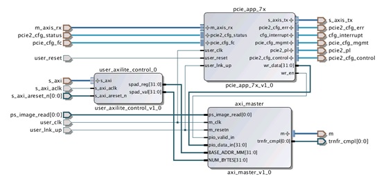
This block is a group of three IPs namely: pcie_app_7x, AXI Master and user_axilite_control as shown in figure below:
The pcie_app_7x module removes the TLP header and extracts the data from the TLP. The software device driver sends 1 DW of data at a time to the PCIe endpoint block.
The AXI Master module implements light weight AXI Memory Mapped interface to suit this application. This block receives 1 DW of data along with data valid signal from the pcie_app_7x block which needs to be written to PS-DDR. The starting address of the location in PS-DDR where the boot image needs to be written can be configured using registers implemented in user_axilite_control block.
The user_axilite_control block gets this information from the PS. The number of bytes to be written and the DDR base address at which the image must be transferred is hardcoded in the modified FSBL code for the current implementation. This base address and number of bytes are written into the scratch pad registers of the user_axilite_control block by Zynq (PS) block which is accessed by the AXI master block through BASE_ADDR_MM and NUM_BYTES signals. The AXI Master will then initiate transfer of the boot image to PS_DDR through AXI High Performance (HP) port. The AXI Master module has logic to monitor the completion of the image transfer using ps_image_read and trnfr_cmpl signals. The trnsfr_cmpl signal is used to indicate that the AXI master has completed writing the entire image into the PS DDR memory. The ps_image_read signal is used to indicate that the FSBL has detected that the transfer is complete and the handoff address (BASE_ADDR_MM) is passed on successfully. This signal is mapped to LED3 on ZC706 board.
PS7:
PS7 block is configured such that the PL fabric clock (FCLK_CLK0) frequency is 250 MHz. One AXI HP port and one GP Port are used to interact with the PL.
AXI GPIO:
It is used to establish the handshake logic between the AXI Master and PS block as shown below. The trnfr_cmpl signal from the AXI Master block is connected to a 1-bit register in AXI GPIO block. The FSBL polls this register until it sees the trnfr_cmpl bit set to ‘1’. FSBL then sets the handoff address to the BASE_ADDR_MM value. The ps_image_read signal value is set to 1 and is written into another AXI gpio register by the FSBL, whose value is polled by the AXI Master block once the image transfer is complete. The FSBL then executes the handoff routine.
Software Implementation
All alterations to FSBL code are carried out in the Xilinx SDK. The SDK comes with the standard FSBL implementation for a Zynq chip, providing a template from which to modify the FSBL code. While the steps necessary to generate a hardware/software package for deployment on a Zynq board will vary based on the medium of deployment, the common components consist of a bitstream to program PL components, generated in Vivado, and an FSBL ELF file created in the SDK itself. An ELF file is an Executable and Linkable Format utilized for software execution.
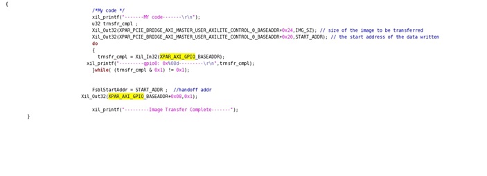
In the current implementation, the standard FSBL is modified to suit the requirement. After all the initialization is done by the FSBL, the FSBL is put in polling mode, waiting for the image to be transferred into PS DDR. Once the FSBL receives the transfer complete signal, it assigns initial DDR address where the image is written to the next handoff address. The code snippet is shown in below:
The above code is placed in the FSBLHandoff function before the handoff is given to the application. The size of the image is defined as a macro IMG_SZ which can be modified by the user and must be written to AXI master user_axilite_control block scratch pad register (0x44A00024) address (spad_val). Also, the DDR address range where the image can be written must be in the range of 0x0010_0000 to 0x3FFF_FFFF, since the lower 1MB in PS-DDR is reserved for OCM. In the current implementation, the start address where image is written is defined by a macro START_ADDR (0x0400_0000). For u-boot image given with package the DDR start address must be 0x0400_0000. For any other applications, it could be any address within the allowable range.
The trnfr_cmpl signal value is polled by constantly reading AXI GPIO register with 0x4120_0000 addresswhose value is asserted by the AXI Master. The ps_image_read signal is asserted when 0x1 value is written in the register another AXI GPIO register with 0x4120_0008 address. This is indicated by the on board LED3. The FSBLStartAddr is assigned the handoff address , 0x0400_0000 in the current implementation and then after the uboot image executes.
Step by Step Instructions
To run the design:
- Download and unzip the design file.
- Insert the SD
- Navigate to sec_boot/ready_to_test folder
- Copy the BOOT.bin file to the SD card and eject the SD
Following steps should be performed on the ZC706 board:
- Set the boot mode selection switches to SD boot mode .
- Insert the SD card in the SD place holder
Following steps to should be run on the host computer:
- Place the ZC706 board in the PCIe v2.1 slot of the host motherboard .
- Connect external power supply to the board .
- Connect one end of the usb-uart cable to the ZC706 board and the other end to control computer.
- Run a serial terminal session on the control computer by selecting the appropriate COM port.
- Power ON the ZC706 board.
- Insert Fedora 16 live DVD in the DVD drive of the host computer and select the boot option to boot from DVD.
$su
- Run the following commands to insert the driver
$make clean
$make
$./make_device
$insmod xpcie.ko
- Navigate to sec_boot/software/app folder. Copy the u-boot binary image to be transferred to PS DDR to this folder.
- Run the application (app.c) by giving the following commands:
$gcc app.c
$./a.out
- After the image transfer is complete and the handoff is given to the u-boot image by the FSBL, the LED3 on board starts glowing indicating that the file transfer is complete.
- After booting the u-boot image, the u-boot prompt can be viewed in the serial communication terminal.
To rebuild the hardware design:
The hardware design can be re built on the control computer usingVivado Design suite. Please follow the below steps:
- Navigate to the location where design zip is present
- Open vivado tcl shell in windows or terminal in linux
- Browse to sec_boot/hardware/vivado/scripts folder
- Setup the Vivado build environment
- Source the sec_boot_over_pcie.tcl script using the following command:
$vivado -source sec_boot_over_pcie.tcl
To generate the BIN file the hardware platform must be imported to the SDK from Vivado. This is done by following the steps below:
- After bitstream generation is complete, click on Open implemented design under Implementation
- Export hardware to SDK along with Bitstream as shown in Figure 5. Select Export Hardware for SDK.
Select include Bitstream option if it is not selected.
To build boot.bin file
The steps to build the boot.bin are as follows:
- After building the hardware platform by following the steps mentioned above, open Xilinx SDK.
- Generate an Application project with the generated hardware platform and standard Zynq FSBL
- Replace the main.c file in the src folder of the Application project with main.c file from sec_boot/software/FSBL_main_code/main.c
- Build the Application project
- Select Xilinx tools in the task bar and choose create Zynq Boot image option.
- Browse to a folder to create a new BIF (output.bif) file
Click on Add icon to add modified FSBL elf file (Bootloader) to the image
Click on Add icon to add datafile i.e generated bitstream of the sec_boot design
- Click on Create Image. This creates a BIN file at the location where output.bif file was created in the first step.
- Rename the BIN file as BOOT.bin and load it in the SD card.
© Copyright 2019 - 2022 Xilinx Inc. Privacy Policy


