Zynq-7000 AP SoC - Performance - Ethernet Packet Inspection - Bare Metal - Redirecting Packets to PL Tech Tip
Zynq-7000 AP SoC - Performance - Ethernet Packet Inspection - Bare Metal - Redirecting Packets to PL Tech Tip
Document History
| Date |
Version |
Author |
Description of Revisions |
| 5/6/2013 |
1.0v |
E. Srikanth |
First Version |
| 2/7/2015 |
2.0v |
Gugulothu Rajesh |
updated with Vivado/SDK 2015.2 tool version |
Introduction
The technical tip described here explains how the Ethernet packet received by the Gigabit Ethernet Interface on the Zynq Processing System can be diverted to the PL for packet inspection. The design used in this tech tip basically comprises of Block RAMs implemented in PL that accepts packets from the PS Ethernet Controller. This design can form the basis for a Hardware Packet Inspection engine that can be implemented in PL.
Designers interested in Packet filtering or Deep packet Inspection of Ethernet Packet can refer to this design to redirect Zynq PS Ethernet data to PL for Hardware Inspection.The concept or theory explained in this tech tip not only applies to PS Ethernet Controller but also can be equally applied for any high speed peripheral having its own DMA controller in the Zynq Processing System.
The design used in this tech tip has been implemented and tested on a ZC702 board.
The design files for this tech tip is located here : Zynq7000AP_SoC_Ethernet_Packet_Redirection_Design.zip
.
Ethernet Data Movement in Zynq Processing System
The Gigabit Ethernet MAC Controller on Zynq Processing System comprises of three blocks.
- MAC Controller
- FIFO(Packet Buffer)
- Ethernet DMA Controller
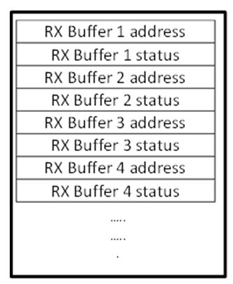
The Ethernet DMA controller is attached to the FIFO to provide a scatter-gather type capability for packet data storage in a Zynq processing system.The Ethernet DMA uses separate transmit and receive lists of buffer descriptors, with each descriptor describing a buffer area in memory. This allows Ethernet packets to be broken up and scattered around the AXI memory space. The data received by the controller is written to pre-allocated buffer descriptors in system memory. These buffer descriptor entries are listed in the receive buffer queue. The Receive-buffer Queue Pointer register of the Ethernet DMA points to this data structure on initialization and uses it to continuously and sequentially to copy the Ethernet packet received in the Ethernet FIFO to Memory address specified in the receive buffer queue.
| Figure 1: Rx Buffer Queue Structure |
In case of Transmit, the data to be transmitted is read from buffers present in system memory. These buffers are listed in the transmit buffer queue. The Transmit Buffer Queue Pointer register of the DMA points to this data structure on initialization and uses it to continuously transmit packets that has been assembled in the address specified in the buffer descriptor present in the transmit buffer queue. More information on the RX and TX Buffer descriptor can be read from the “16.3.5 Configure the Buffer Descriptors “section in the Zynq-7000 Technical reference manual(UG585). As described above, in the current Zynq Processing System the Transmit and receive buffer descriptors are initialized in the Ethernet driver before the Ethernet Hardware is enabled in the software.
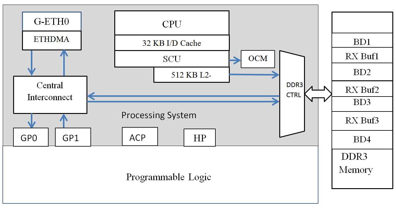
When an Ethernet Packet is received, the Ethernet DMA uses the address in the RX Buffer descriptor to push the packet that has been buffered in the Packet Buffer on Ethernet interface to DDR3 memory, via the central interconnects. In this case the data is not cached and is directly passed on the DDR3 memory.
In case of transmit the Ethernet DMA uses the address in the TX Buffer descriptor to pull data from DDR3 Memory, through the central interconnect and finally to the ETH0 Interface.
- Data Receive Path: ETH0 à ETH0 DMA (32-bit)à Central Interconnectà DDR3 Memory Controller (64-bit AXI).
- Data Transmit path: DDR3 Memory Controller (64-bit AXI) à Central Interconnectà ETH0 DMA (32-bit) àETH0
| Figure 2: Ethernet Data Movement |
Implementation
| Implementation Details |
|
| Design Type |
PS & PL |
| SW Type |
Standalone |
| CPUs |
1 ARM Cortex-A9 666MHz |
| PS Features |
|
| PL Cores |
Two PL Block RAMS Used |
| Boards/Tools |
ZC702 |
| Xilinx Tools Version |
VIVADO / SDK 2015.2 |
| Other Details |
. |
Setup and procedure for redirecting the Ethernet Packet to the PL for Packet Inspection.
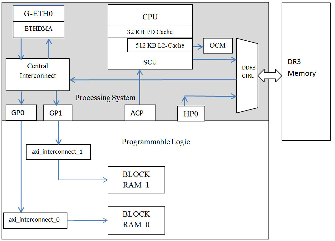
In this tech tip, the Zynq Processing system uses programmable logic (PL) BRAMS for storing packet control and packet data information coming from PS MAC. The first Block RAM in the design is connected to General Purpose AXI Master (MAXI_GP0) port 0. The MAXI _GP0 port can viewed as a separate control path and can be used to access any control information of any IP implemented in PL. This system utilizes this Block RAM to save the actual memory address programmed in the Buffer Descriptor before redirecting the packet to the PL.
The second Block RAM is connected to General Purpose AXI Master (MAXI_GP1) port 1 via the AXI interconnect. The MAXI _GP1 port provides the data path to store the received Ethernet packets into two memory regions in the Block RAM connected to it. The Block RAM has been logically organized to handle two consecutive Ethernet packets at locations 0x80000000 and 0x80001000 respectively.
| Address Map |
|||
| Base_Address |
Size |
Interface |
|
| Block RAM 0 |
0x40000000 |
16K |
S_AXI |
| Block RAM 1 |
0x80000000 |
16K |
S_AXI |
Block Diagram
A simplified block diagram of the connections to Zynq PS and Ethernet Packet Processing unit is as shown below.
| Figure 3:Zynq Interconnections to the Block RAMs |
Software Implementation
The test program provided in this tech tip is an updated code of the Ethernet Peripheral Test template provided in the SDK tool. In the Standalone BSP Ethernet driver, the transmit and receive buffer descriptors start addresses are allocated in the OCM. This has been done because for the PS Ethernet the Buffer Descriptors need to be placed in uncached memory.#define RX_BD_LIST_START_ADDRESS 0x0FF00000
#define TX_BD_LIST_START_ADDRESS 0x0FF10000
The Ethernet Test Peripheral Program assembles a sample IPV4 Ethernet Packet in the Transmit buffer, and starts the Ethernet DMA to transmit the Ethernet packet on the receive interface. The Transmitted packet is internally looped backed by the Ethernet PHY to the receive Buffer of the Ethernet MAC Controller. The Ethernet Receive DMA then copies the packet from the MAC Receive FIFO to the address specified in the Receive Buffer Descriptor and then updates the packet status in the status word of the Receive Buffer Descriptor.
| Figure 4: Example Rx Buffer Descriptor Queue |
So, in order to push the data to MAXI GP1 port, The Ethernet DMA Descriptors in the test program has been modified to enable the data to be forwarded to the MAXI_GP1 port. This corresponding redirection has been achieved by preserving the address of the memory address that has been allocated by the OS in Block RAM 0 and then reprogramming the Receive Buffer Descriptor with the address of the Block RAM 1 present in the PL. This process has to be done for all the Receive Buffer descriptors in the ring to redirect each and every packet to the Programmable Logic.
In the current implementation the Block RAM 1 has been logically divided into two regions i.e. 0x80000000 and 0x80001000 for receiving two consecutive packets. So in order to redirect the packet at the above two addresses specified (0x80000000, 0x80001000) the addresses for each of the Receive Buffer descriptor can be alternately programmed as shown below.
| Figure 5:Modified Buffer Descriptor Queue |
The below software snippet is provided as an example which saves the addresses in the queue and reprograms the queue to store two consecutive packets in the Block RAM for packet inspection.
#define BUFFER_DESC_MEM 0x40000000

#define PACKET_BUFFER_0 0x80000000

#define PACKET_BUFFER_1 0x80001000


......


/* Section of code in ppu_test function


/* Save the addresses in Buffer Descriptor in OCM to Block RAM in PL

 * Set up the Buffer Descriptor in OCM to redirect packets to PL before starting the EMAC device*/

 for(bd_index=0;bd_index<RXBD_CNT; bd_index++)

 {

 if((bd_index%2) == 0)

 {

 //Copy Buffer address from 0x0FF0_0000 to 0x4000_0000

 *(u32*)(BUFFER_DESC_MEM + (bd_index * 8) ) = &&RxBuffer[bd_index][0];

 printf("\r\nRxBuffer Addr in BD%d: %8x is saved in PL \r\n", bd_index, &&RxBuffer[bd_index][0]);

 printf("\r\nPacket will be redirected to 0x80000000 \r\n");


 //Reinitialize Buffer address at 0x0FF0_0000 to 0x8000_0000

 *(u32*)(RX_BD_LIST_START_ADDRESS + (bd_index * 8)) = PACKET_BUFFER_0;


 }

 else

 {

 //Copy Buffer address from 0x0FF0_0000 to 0x4001_0000

 *(u32*)(BUFFER_DESC_MEM + (bd_index * 8) ) = &&RxBuffer[bd_index][0];

 printf("\r\nRxBuffer Addr in BD%d: %8x is saved in PL\r\n", bd_index, &&RxBuffer[bd_index][0]);

 printf("\r\nPacket will be redirected to (0x80001000)\r\n");


 //Reinitalize Buffer address at 0x0FF0_0000 to 0x8000_1000

 *(u32*)(RX_BD_LIST_START_ADDRESS + (bd_index * 8)) = PACKET_BUFFER_1;

 }

 }
Step by Step Instructions
ZC702 Board Setup
- Connect the board to the power cable
- Connect a Xilinx Platform cable USB II cable or digilent cable between the Windows Host machine and the Target board with the following details, based on your cable type.
| CableType |
Bit1 |
Bit2 |
| Xilinx Platform Cable USB II |
1 |
0 |
| Digilent Cable |
0 |
1 |
- Connect a USB cable to connector J17 on the target board with the Windows Host machine. This is used for USB to serial transfer.
- Power on the ZC702 board using the switch indicated in Figure 7.
Figure 6:ZC702 Board Power Switch
Generating the Hardware Design
- Copy the Zynq7000AP_SoC_Ethernet_Packet_Redirection_Design.zip file to your hard drive and unzip the file to C drive.
- Open the Xilinx Vivado 2015.2 tool
- Select Open Project to open the existing project.
- Browse to the C:\Zynq7000AP_SoC_Ethernet_Packet_Redirection_Design\HW\project” folder where the Vivado project is present as shown in the Figure 7.
- Select the project.xpr file and select ok as shown in the figure 7.
Figure 7: Opening existing Vivado project - It will create the block design in the Vivado IP integrator.Open the block design by selecting Open Block Design option under the IP integrator sub menu of Flow Navigator.Verify the address mapping of block RAM's in the Address Editor.
Figure 8:Project View - Generate the bit stream by selecting Generate Bitstream option under the Program and Debug sub menu of Flow Navigator.Once the Bit stream generation is completed ,a confirmation wizard for opening implemented design will appears,click OK in that.
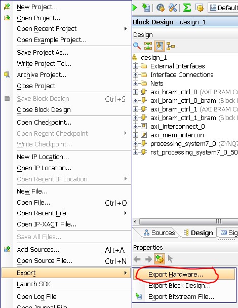
- After opening the implemented design ,Export the hardware design to SDK work space by following below step.
- Select File > Export Hardware as shown in the below figure.
Figure 9: Exporting hardware - Check the Include bitstream check box in the Export Hardware wizard and click OK.
- Now launch the SDK by selecting File > Launch SDK and select OK in the Launch SDK wizard.It will launch the SDK and creates the SDK work space in the same work space where Vivado hardware project is created.
- After launching the SDK work space , close the SDK welcome screen.
- In SDK create a new application project. Select File > New > Application Project. The New Project wizard opens
- Use the information in the table below to make your selections in the wizard screens.
- Click Finish.
- The New Project Wizard closes and SDK creates the packet_redirect project and the packet_redirect_bsp BSP project under the project explorer. SDK also automatically compiles the project and generates the BSP.
- In the Project Explorer tab, expand the packet_redirect project, right-click the src directory, and select Import to open the Import dialog box.
- Expand General in the Import dialog box and select File System.
- Click Next.
- Add all the files present in “C:\Zynq7000AP_SoC_Ethernet_Packet_Redirection_Design\sw\srcs\” directory and click Finish.
Figure 10:Importing the sources to the empty project - SDK automatically builds the application and displays the status in the console window
- Expand the packet_redirect àsrc and open the xemacps_example_intr_dma.c.
- Observe the ppu_testfunction at line numer 1099.After reviewing the code, close the file.
- Select Xilinx Tools à Program FPGA.
Figure 11: Programming FPGA - Make sure that bit file selected in the Bitstream option is correct.
- Click on Program to download the bitstream to the ZC702 board.
- Open a Serial Terminal (Like Hyperterminal or Teraterm) configured at following settings. Baudrate: 115200 No of bits: 8 Parity : 1 Flow Control : NONE
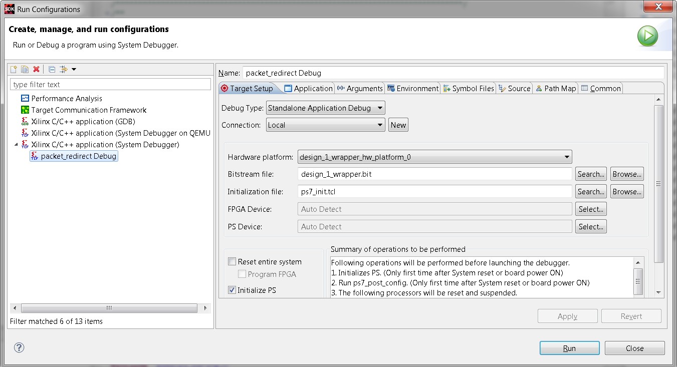
- In the Project explorer view of the SDK tool, Right click “packet_redirect ” folder and select Run As à Run Configurations. This will launch the Run Configurations dialog.
- In the run configurations dialog , Double click on the Xilinx C/C++ ELF application (System Debugger) to create a new configuration as shown below
Figure 12:Creating a New Run Configuration - Select the packet_redirect_Debug configuration and click on Run.
- Observe the message in the Serial console to view the results.
Expected Results
- The first section of the test program displays the actual addresses programmed by the Ethernet driver. The Packet Redirect code will replace the actual buffer addresses with the addresses of the BRAMs of the Packet Processing Unit.
Figure 13:Test Results displaying the modification of the Buffer descriptors - The second section in the ppu_test function compares the transmitted packet with the packet received in Block RAM in the PL for its data integrity.
- Here we see that there are no errors, indicating no data corruption has occurred.
- The last section displays the content in the PL Block RAM for manual inspection. Here we see there are no errors and no data corruption has happened.
How to Expand
Designers interested in Packet filtering or Deep packet Inspection of Ethernet Packet can adopt this method to redirect the Zynq PS Ethernet data to PL for Hardware Inspection.Designers can alternatively move the Ethernet Packets to L2 Cache by redirecting the Ethernet Packet to the Programmable Logic and develop a custom design which pushes the the data to l2 Cache via the Zynq ACP port.
The design provided in the Tech Tip Redirecting Ethernet Packets to L2 Cache via ACP provides a method to redirect Ethernet Packets to ACP via PL with some limited packet inspection perfomed in Programmable Logic.
Appendix A:File Description in Zynq7000AP_SoC_Ethernet_Packet_Redirection_Design.zip
Directory Structure is
- Zynq7000AP_SoC_Ethernet_Packet_Redirection_Design\HW\project:
- Vivado harware design project directory: Contains the supported design files for the tech tip.
- Zynq7000AP_SoC_Ethernet_Packet_Redirection_Design\sw\srcs
- Contains Source files for the SDK project.
- testperiph.c: Top level application software running the test programs for Interrupt and PS Ethernet
- xemacps_example_intr_dma.c: Application program for testing single Ethernet loop back program.
- Contains other supporting application files required for testing Ethernet hardware.
- Contains Source files for the SDK project.
© Copyright 2019 - 2022 Xilinx Inc. Privacy Policy

