Zynq AMS Post Processing in PL App Note
- Confluence Wiki Admin (Unlicensed)
- Terry O'Neal (Unlicensed)
Table of Contents
1 Introduction
This page provides instructions on how to build various components of the ZC702 AMS Post Processing using Sensor Linearizer, FIR filter and Decimator IP in Zynq-7000 SoC Programmable Logic and how to setup the hardware platform and run the design on the ZC702 Evaluation Kit. The ZC702 Evaluation kit is based on a XC7Z020 CLG484-1 Zynq-7000 SoC device. For additional information, refer to XAPP12031.1 About the AMS Post Processing Application Note
Most systems need to be able to interact with the real world for the purpose of monitoring and controlling it. To allow this to happen, systems contain sensors that translate real-world stimuli, such as light, heat, and sound, into analog electrical signals. The analog outputs of these sensors need to be processed and digitized so that the appropriate information can be presented to the digital controller or processor. The analog processing and conditioning of the sensor output is done in many different ways, depending on factors such as the accuracy requirement and the type of sensor used. Common analog functions include:
• Level Translation (Bipolar to Single-Ended)
• Gain/Attenuation
• Bandwidth Limiting/Filtering/Noise Reduction
• Gain and Offset Error Cancellation
• Linearization
As most systems process digital information, an analog-to-digital converter (ADC) is required to digitize the processed sensor output. These ADCs come in many forms and are typically defined by their resolution and speed. ADCs are now also integrated into microcontrollers and FPGAs, such as the XADC, which can be found in all Xilinx's 7 series FPGAs and SoCs. ADC speeds have increased significantly over the years due to process scaling. It is now relatively inexpensive to buy ADCs with sample rates in the range of 1 MSPS and above. This increase in speed, together with digital signal processing, can be leveraged to enhance the performance of the solution.
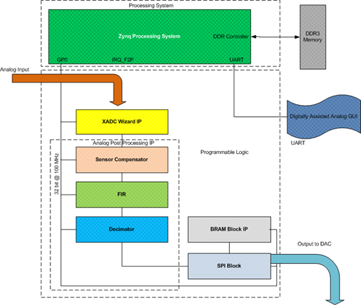
The block diagram of the design is shown in Figure below. The design composes of a control processor and the analog post processing IP implemented on Zynq-7000 SoC Programmable Logic (PL). The analog post processing IPs use the DSP48 embedded macros available in the PL.
The design has Cortex-A9 multicore processor in Zynq-7000 Processing System that acts as a control processor and initializes and configures the different peripheral blocks used in the design.
1.2 Package Content
The XAPP1203 package contains the following:
- XAPP1203 IPI based Hardware Design Files
- XAPP1203 Application C code
- Pre-built SD images for out-of-box user experience
- Readme file
The following Figure shows the directory structure tree.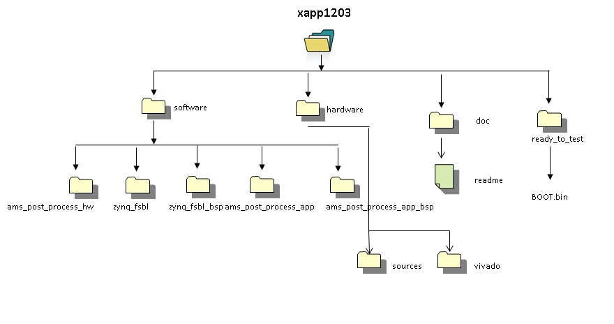
2 Prerequisites
- The ZC702 Evaluation Kit ships with the version 2013.4 Device-locked to the Zynq-7000 XC7Z020 CLG484-1 device and all required licenses to build the application note.
- A Linux/Windows development PC with Vivado 2013.4 Vivado Design Suite installed
- A Linux/Windows development PC with Xilinx SDK 2013.4 version installed
- TeraTerm/HyperTerminal application for communicating with the Zynq-7000 AP SoC design
3 Building the Hardware Design
This section explains the steps required to implement the Hardware Design using Vivado Design Suite, 2013.4.
- On Windows 7, browse to Start > All Programs > Xilinx Design Tools > Vivado 2013.4 > Vivado 2013.4 Tcl Shell
- On Linux, Vivado will be invoked automatically by the Tcl script provided with the XAPP1203
- Browse to xapp1203/hardware/vivado/scripts folder
- On the Tcl Shell or the command prompt, type the following command
$ vivado -source create_project.tcl
The above step invokes the Vivado GUI and opens the Vivado Project and the Block Diagram design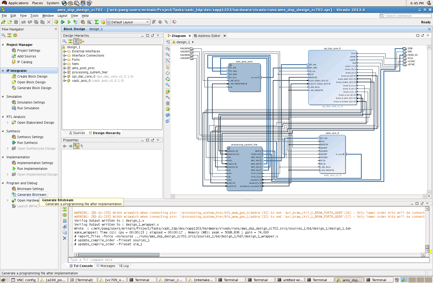
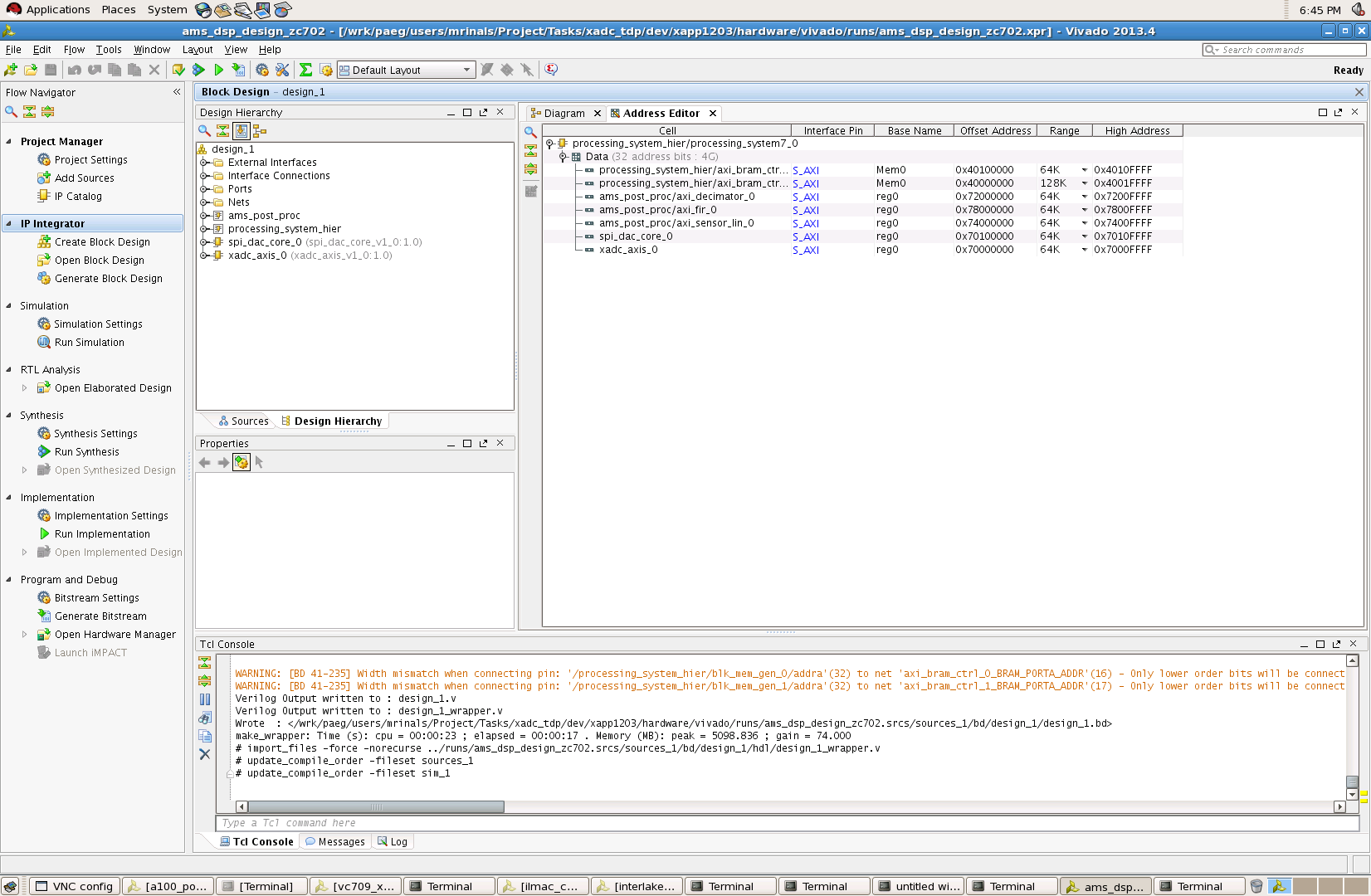
- Edit the slave addresses of the peripherals as required in the Address Editor tab:
- Click on Generate Bitstream Option in the left panel of the Vivado GUI
The above step generates the bitstream of the design.
- Click on the Open Implemented Design dialogue box once the bitstream generation completes
- Click on File->Export HW-> Export HW for SDK option

The user can import the AMS post processing hierarchical block containing Sensor Linearizer IP, FIR filter IP and the Decimator IP to their design by typing the following command in the Vivado GUI Tcl prompt:
source ams_post_proc_hier.tcl
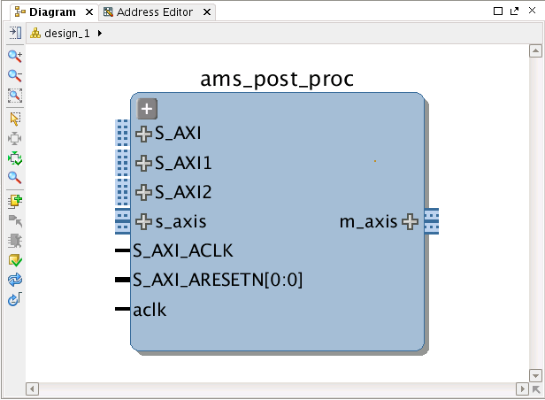
Note that the user has to create a Vivado project before importing the Tcl file that instantiates AMS post processing hierarchical design.
The user needs to make the necessary connection to the below interface ports:
| Interface Name | Description | Connection |
| S_AXI | AXI4 Lite slave interface for FIR filter IP This interface is used for configuring the IP and needs to be connected to an AXI4 Interconnect | Mxx port of AXI4 Interconnect IP |
| S_AXI1 | AXI4 Lite slave interface for Decimator IP This interface is used for configuring the IP and needs to be connected to an AXI4 Interconnect | Mxx port of AXI4 Interconnect IP |
| S_AXI2 | AXI4 Lite slave interface for Sensor Linearizer IP This interface is used for configuring the IP and needs to be connected to an AXI4 Interconnect | Mxx port of AXI4 Interconnect IP |
| s_axis | AXI4 Stream Interface for data. The slave interface needs to be connected to the AXI4 Stream master interface of XADC Wizard IP | m_axis interface of XADC Wizard IP |
| S_AXI_ACLK | Clock port for AXI4 Lite Interface | Mxx_ACLK of AXI4 Interconnect IP |
| S_AXI_ARESETN | Reset port for AXI4 Lite Interface | Mxx_ARESETN of AXI4 Interconnect IP |
| aclk | AXI4 Stream Interface clock | ACLK port of XADC Wizard IP |
4 Building the FSBL
This section explains the steps for building the FSBL.
- On Windows 7, select Start > All Programs > Xilinx Design Tools > SDK 2013.4 > Xilinx SDK 2013.4
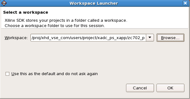
- On Linux, enter xsdk at the command prompt.In the Workspace Launcher window, click Browse and navigate to xapp1203/software, then click OK. Close the welcome screen
- Click on File -> New -> Application project

- Select ZC702 predefined Hardware Platform and click on Next.
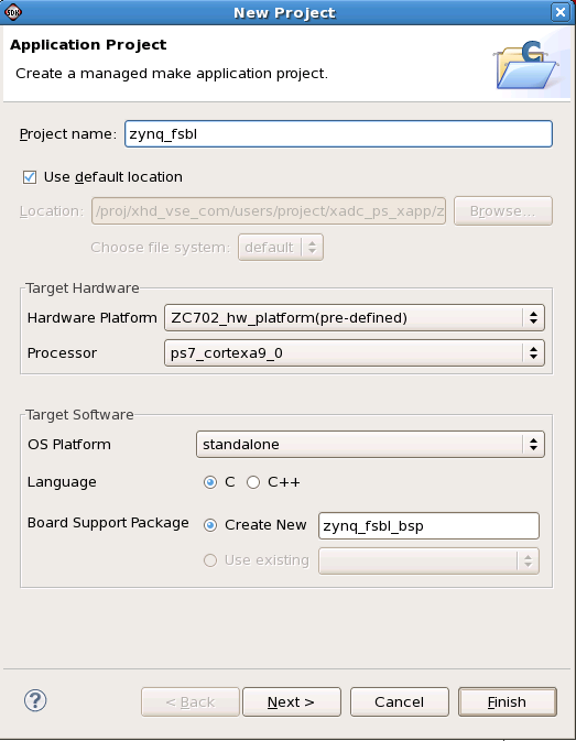
- Select Zynq FSBL and click on Finish
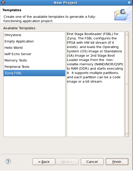
The final step will create the Zynq FSBL elf file
5 Building the Application Project
This section details about the steps required building the application
- On Windows 7, select Start > All Programs > Xilinx Design Tools > SDK 2013.4 > Xilinx SDK 2013.4
- On Linux, enter xsdk at the command prompt.In the Workspace Launcher window, click Browse and navigate to xapp1203/software, then click OK. Close the welcome screen
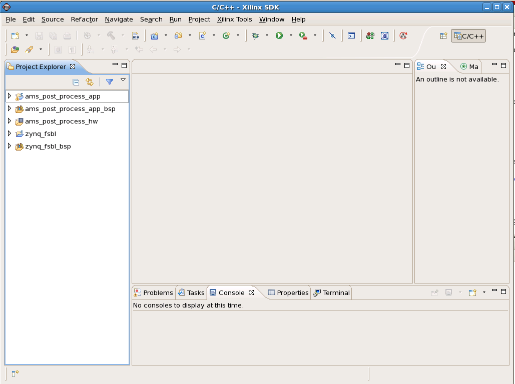
- Xilinx SDK shows the application project and the board support package as shown in the figure below
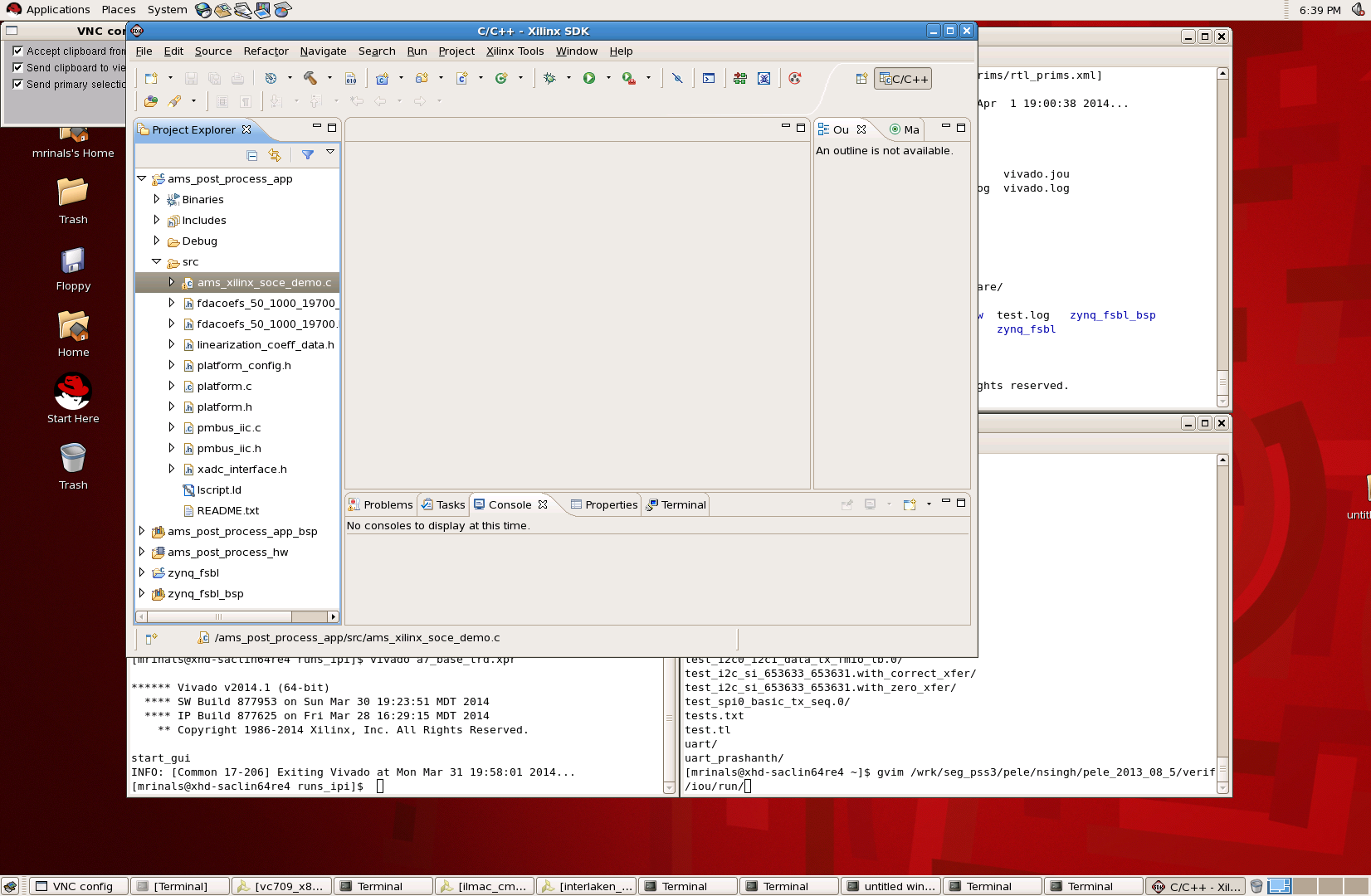
- Click on ams_post_process_app->src->ams_xilinx_soce_demo.c file
- Edit the application file as required and rebuild the project
6 Hardware Setup Requirements
1. The ZC702 evaluation board with the XC7Z020 CLG484-1 part2. XAPP1203 zip file containing the design files
2. Internet Explorer version 8.0 or aboveAMS101 evaluator card
3. Optional signal generator to test externally applied analog signal
4. Mini USB cable
5. Class 4 equivalent SD card
6. A control PC
7 References
- User Guide for XAPP1203
- Documentation for Zynq-7000 AP SoC
- Documentation for ZC702 Evaluation Kit
- Main Xilinx wiki
Related content
© Copyright 2019 - 2022 Xilinx Inc. Privacy Policy