Zynq-7000 AP SoC - RealTime - InterruptLatency Reference Design and Demo Tech Tip
Table of Contents
Document History
| Date | Version | Author | Description of Revisions |
|---|---|---|---|
| 9/30/2014 | 0.1 | Upender Cherukupally | initial Draft |
| 1.0 | Rutuja Chavan | Added FreeRTOS design and updated to version 2015.4 |
Summary
The interrupt latency is the time elapse when an interrupt is generated to when the interrupt source is acted on i.e. duration between an interrupt generation/external event and CPU core branches to first instruction of the interrupt service routine. In real time systems, the interrupt latency plays a major role in the determinism and overall system response to a real time event. The interrupt latency depends on different factors like interrupt controller implementation, low level software architecture, operating systems, middle-ware stacks, device or peripheral specific interrupt handling requirements, priority of the interrupt and interrupt handler implementation.
The Zynq-7000 AP SoC has an inbuilt hardened interrupt controller called generic interrupt controller (GIC). The dual ARM Cortex A9 processing cores handle the generic peripheral interrupts in IRQ and FIQ modes. The GIC is a centralized resource for managing interrupts sent to the CPUs from the PS and PL. The controller enables, disables, masks, and prioritizes the interrupt sources and sends them to the selected CPU or both CPUs. In addition, the controller supports security extension for implementing a security-aware system.
This reference design and demo shows
- The interrupt latency (max, min, ave and jitter) information for a PL peripheral interrupt
- Using the Private Peripheral Interrupt (PPI) and Shared Peripheral Interrupt (SPI) interrupts
- Different options like moving the ISRs to OCM, DDR, cached and non-cached memory locations etc in case of bare metal software
- Creating the page faults to have a real time scenario and know the maximum/worst case interrupt latency with Linux OS
Implementation
| Implementation Details | |
| Design Type | PS and PL |
| SW Type | Zynq-7000 AP SoC Linux AMP |
| CPUs | 2 ARM Cortex-A9: Core 0 Linux and Core 1 Baremetal/FreeRTOS |
| PS Features |
|
| PL Cores | AXI Timer Soft Cores to generate PL to PS interrupts |
| Boards/Tools | ZC702 kit |
| Xilinx Tools Version | Vivado 2015.4 or latest |
| Other Details | - |
| Files Provided | |
| zynqInterrupts.zip | Archived file contain the following folders:
|
This TechTip covers the following topics:
- Zynq-7000 AP SoC Generic Interrupt Controller overview
- Interrupt latency measurement design details
- How to create the HW project using the Vivado tool
- How to create the SW project for the: Linux AMP where Core 0 running Linux software, Core 1 running bare metal and FreeRTOS software
- Running the Demo: Linux AMP with Baremetal/FreeRTOS interrupt latency demo
Zynq-7000 AP SoC Generic Interrupt Controller Overview
The Generic Interrupt Controller (GIC) is a centralized resource for managing interrupts sent to the CPUs from the PS and PL. The controller enables, disables, masks, and prioritizes the interrupt sources and sends them to the selected CPU (or CPUs) in a programmed manner as the CPU interface accepts the next interrupt. In addition, the controller supports security extension for implementing a security-aware system.The PS general interrupt controller (GIC) supports 64 interrupt input lines that are driven from other blocks within the PS or the PL. Six of the 64 interrupt lines are driven from within the APU. These include L1 parity fail, L2 interrupt (all reasons), and PMU (performance monitor unit) interrupt.
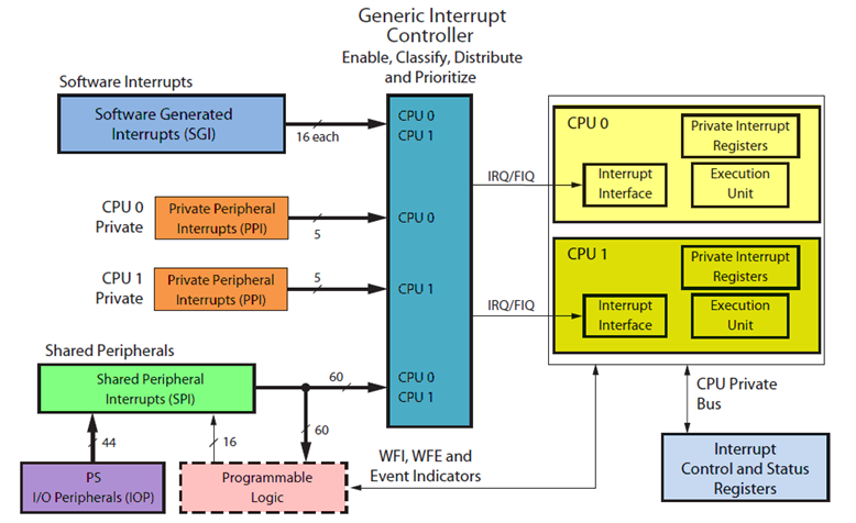 |
| Figure 1: GIC Block Diagram |
The interrupts on the GIC are divided in two three major blocks: Software Generated interrupts (SGIs), Private Peripheral Interrupts (PPIs) and Shared Peripheral Interrupts (SPIs).
Interrupt numbers ID0-ID31 are used for interrupts that are private to a CPU interface and are banked in the distributor. A banked interrupt is one where the distributor can have multiple interrupts with the same ID. A banked interrupt is identified uniquely by its ID number and its associated CPU interface number.
The banked interrupt IDs
- ID0-ID15 SGIs
- ID27-ID31 PPIs
Interrupt numbers from ID32-ID92 are the SPIs to which all the interrupts of the PS-shared peripheral interrupts are connected. From these, 16 of the interrupt sources (ID61 to ID68 and ID84 to ID91) can be driven from the programmable logic.
The GIC collects interrupts from various sources and distributes these interrupts to each of the ARM cores. Each ARM core accepts two different types of interrupts: nFIQ interrupts from secure sources and nIRQ interrupts from either secure or non-secure sources.
The interrupt distributor holds the list of pending interrupts for each Cortex-A9 processor. It selects the highest priority interrupt before issuing it to the Cortex-A9 processor interface. Interrupts of equal priority are resolved by selecting the lowest ID.
The PS to PL and PL to PS interrupts are need to be enabled and mapped to the interrupt lines as per the design requirements. Below figure is an example of PL to PS interrupt configuration in Vivado IPI Zynq block design GIC customization used in this demo:
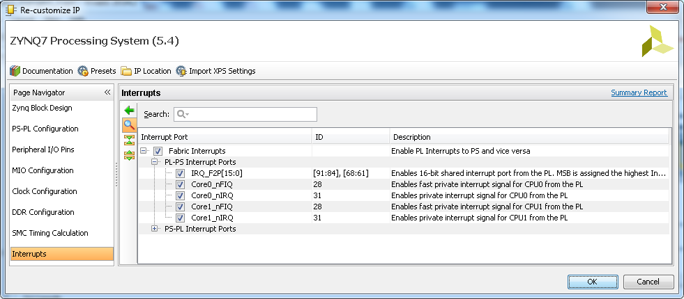 |
| Figure 2: PL to PS Interrupts configuration |
The prioritization logic is physically duplicated to enable the simultaneous selection of the highest priority interrupt for each Cortex-A9 processor. The interrupt distributor holds the central list of interrupts, processors, and activation information and is responsible for triggering software interrupts to processors. For more details refer the Zynq-7000 AP SoC TRM (UG585).
Reference Design Block Diagram
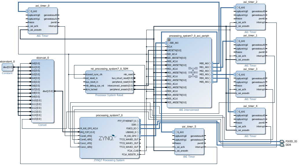
Figure 3 illustrates the functional blocks of the Zynq-7000 AP SoC interrupt latency measurement hardware design. The PL is instantiated with the six AXI timers, connected to GP0 for the control registers access or programming, the interrupt lines form these timers are connected to:
- Core 0 FIQ,
- Core 0 IRQ,
- Core 1 FIQ,
- Core 1 IRQ and
- shared peripheral interrupt line 91.
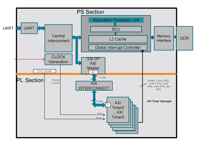 |
| Figure 3: Interrupt latency measurement design block diagram |
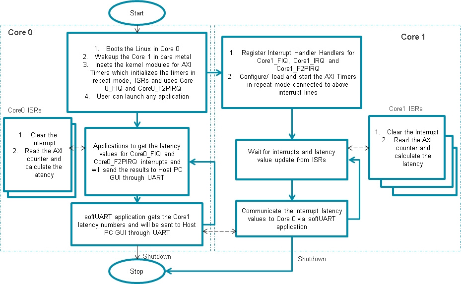 |
| Figure 4: Software Flow diagram of the Linux AMP Interrupt Latency measurement design |
Interrupt latency measurement details
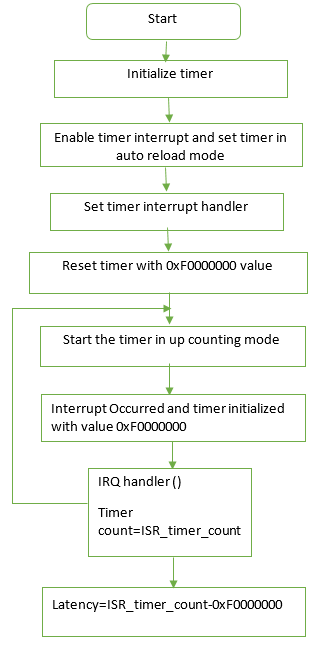 |
| Figure 5: Flow chart of interrupt latency measurement |
This section is required if you want to build the design for new tool versions or kernel release. If you want to run the pre-build images then refer the Running the Demo section
- Launch the Vivado IDE Design Tool:
- Start > Xilinx Design Tools > Vivado 2015.4 > Vivado 2015.4 or latest
- For Linux, enter Vivado at the command prompt
- Create New Project in launch window, a new Vivado project wizard will open and then click Next
- In the Project Name dialog box, type the project name (e.g. Zynq_PLInterrupts) and browse for the project location. Ensure that Create project subdirectory is checked, and then click Next.
- In the Project Type dialog box, select RTL Project and ensure that Don’t specify the sources at this time is checked then click Next.
- In the Default Part dialog box select Boards and choose ZYNQ-7 ZC702 Evaluation Board or ZYNQ-7 ZC706 Evaluation Board. Make sure that you have selected the proper Board Version to match your hardware because multiple versions of hardware are supported in the Vivado IDE and then Click Next.
- Review the project summary in the New Project Summary dialog box before clicking Finish to create the project.
- In the Project Manager wizard under IP Integrator select Create Block Design, enter the design name or leave default (design_1) in the Please specify name of the block design pop-up window and select ok
- In the desing_1 drawing view select Add IP button and select Zynq7 Processing System in the next pop-up search window
- Select Run Block Automation and /processing_system7_0
- In next Run Block automation pop-up make sure that apply board preset is checked and select ok
- In next window select and connect the clock inputs
- Add the 6 AXI Timer IPs using the Add IP button in the design_1 drawing view and run the Run Block Automation and select the defaults in following options
- Enable the PL to PS Interrupts by using the GIC configuration, this can be done by double-clicking the Zynq7 Processing system block and select the GIC component in the block diagram and enable the interrupt as shown in the following Figure 5.1 and then click ok.
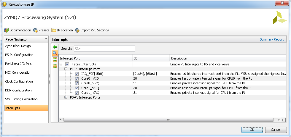 |
| Figure 6.1 Enabling the PL to PS interrupts for both the Cores |
Connect the AXI Timer interrupt lines to the Interrupts lines enabled in the above step and block diagram looks as following Figure 6.2
Interrupt latency block diagram Click on Generate block design and generate in next pop-up under the Flow Navigator
- Once generation is successful create the HDL wrapper and select the default option in next window pop-up
- Select Generate block design in the IPI navigator
- User can also create HW block design using reference file shared in this tech tip.
- source design_1_bd.tcl file, which will create block design. design_1_bd.tcl is under "<sdk_workspace>/design_1_wrapper_hw_platform_0" folder under reference design files.
- Run generate bitstream in vivado tool.
- From file menu Export Hardware for SDK once the HDL Wrapper is created
- Once Export hardware is done, launch the SDK from the file menu
Application software development:
This section describes about the application development and creation of the booting image. This booting image is to boot the ZYNQ device and run the application on CPU1. If user wants to skip this section and jump to Application Execution, then prebuilt image (BOOT.bin) is included and located in the directory Zynq_intr_latency/LinuxAMP/Images/Core0Linux_Core1Baremetal_SD and it can be used.
After SDK launch, the projects can be imported to use the provided reference design files.
- Select File -> Import to open an import wizard.
- Select General > Existing Projects into Workspace in the import wizard.
- Select Achieve file and specify the location where the software applications are stored.
- The import wizard displays a list of projects that are available to import. This list Includes
- Build each of the above imported projects.
- For building the Linux kernel modules add the Linux source directories in the /drivers/char/ folder and update the make files at /drivers/char/ by adding: obj-m += ./newly added folder names and build the kernel, if you plan to build the FIQ kernel module then enable FIQ in arch/kconfig file of the kernel source
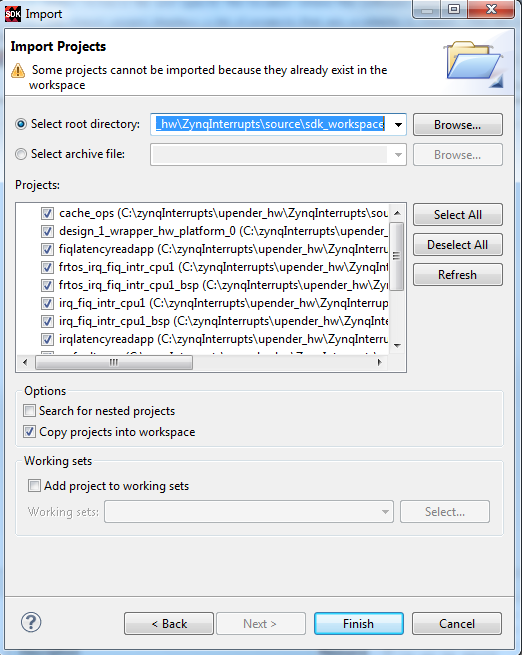 |
| Figure 6-3: Application software development |
Generating Boot File:
- In SDK, select Xilinx Tools > Create Boot Image. The Create Zynq Boot Image wizard opens.
- Provide the zynq_fsbl.elf , Bit stream file and Application elf(u-boot.elf and baremetal/FreeRTOS.elf) files. Please refer the bootimage.bif shared under reference files.
- Provide the output folder name in the Output Folder tab
- Click Create Image.
 |
| Figure 6-4: Generating Boot file |
Linux AMP Interrupt latency demo:
Step 1:There are two designs (Baremetal and FreeRTOS application) shared under reference design folder. If user wants to check baremetal application latency then copy the contents from ..Zynq_intr_latency/zynq_intr_latency_v_2015.4/LinuxAMP/Images/Core0Linux_Core1Baremetal_SD to the SD card. And if user wants to check FreeRTOS application interrupt latency, copy the contents from .. Zynq_intr_latency/zynq_intr_latency_v_2015.4/LinuxAMP/Images/Core0Linux_Core1FreeRTOS_SD to the SD card.
Step 2: ZC702 Kit setup:
- Connect the mini-USB cable to the USB-UART connector/ mini-B receptacle on the board to the PC,
- Connect the board power supply, insert the SD card in the SD card slot,
- Make sure the board is in SD boot mode (SW 16: 3 & 4 to high)
- Power cycle the board and note the COM port to switch the USB-UART is connected
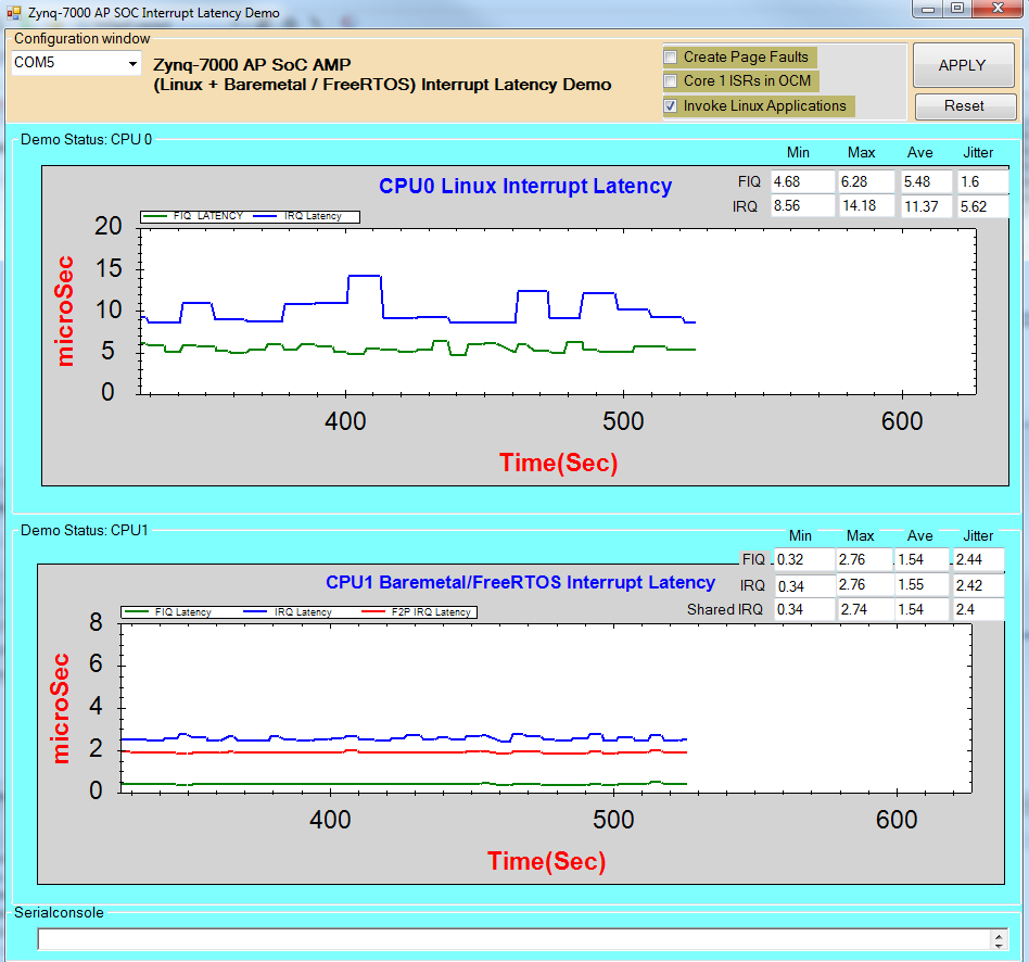
Step 3: Launch the GUI executable from ..zynq_intr_latency/zynq_intr_latency_v_2015.4/LinuxAMP\Images/GUI/ and select the COM port to which the ZC702 board is connected
Step 4: Press enter key at the bottom serial console window in GUI or power cycle the ZC702 board
Step 5: Select the ‘APPLY’ button once it is enabled. This will show the different graphs related to the interrupt latency and update the status text boxes with minimum, maximum, average and jitter information related to corresponding interrupt line.
Step 5: There are dynamic configuration options besides the APPLY button, you can select or de-select these options to see the variations in the interrupt latency. To get these selection to the ZC702 board you need to select the APPLY button again for any change in the configurations
Achieving better interrupt latency:
To Achieve better interrupt latency core 1 ISR function is added into OCM(On Chip Memory) to get faster memory access. OCM address used for the reference design is 0xFFFF0000. Following steps are performed to execute core 1 ISR in OCM
Step 1: Created memory section under application linker script for OCM. Add following code in linker script.
.ocm_isr_tbl : {
ocm_isr_tbl_start = .;
*(.ocm_isr_tbl)
ocm_isr_tbl_end = .;
} > ps7_ram_1_S_AXI_BASEADDR
Step 2: Modified application function to get execute under OCM as shown in below example. LowIrqHandler_OCM is ISR function in application, add attribute to execute in OCM.
LowIrqHandler_OCM(void *CallbackRef) attribute((section(".ocm_isr_tbl")))
Step 3: FSBL creates partitions to execute into DDR memory, Modified partiions in FSBL to get it execute under OCM.
Expected Results:
These numbers are purely based on the design and implementation of the over all system. The below listed numbers are as per the example design provided by this techtip. All the numbers are in micro-seconds.
Design: Linux + Baremetal AMP Interrupt latency
Core 0 Linux Interrupt latency| CPU 0 | Normal execution | Page fault | Application invocation | |||
| FIQ | 2.76 | 6.06 | 5.56 | |||
| IRQ | 5.58 | 11.5 | 9.7 |
Core 1 Bare metal Interrupt latency
| CPU1 | Normal execution | ISR in OCM | ||
| FIQ | 0.76 | 0.4 | ||
| IRQ | 1.58 | 1.9 | ||
| F2P_IRQ | 2.5 | 2.46 |
 |
| Figure 7-1: Linux + Baremetal AMP interrupt latency result |
Design: Linux + FreeRTOS AMP Interrupt latency
Core 0 Linux Interrupt latency| CPU 0 | Normal execution | Page fault | Application invocation | |||
| FIQ | 2.74 | 5.62 | 5.1 | |||
| IRQ | 5.7 | 10.92 | 12.3 |
Core 1 FreeRTOS Interrupt latency
| CPU1 | Normal execution | ISR in OCM | ||
| FIQ | 0.72 | 0.34 | ||
| IRQ | 1.5 | 1.84 | ||
| F2P_IRQ | 2.38 | 2.34 |
Application software development
 |
| Figure 7-2: Linux + FreeRTOS AMP interrupt latency result |
© Copyright 2019 - 2022 Xilinx Inc. Privacy Policy