Zynq-7000 AP SoC - AMP Solution without External Memory Tech Tip
Zynq-7000 AP SoC - AMP Solution without External Memory Tech Tip
| Date |
Version |
Author |
Description of Revisions |
| 8/11/2014 |
0.1 |
Yashu Gosain |
initial version |
| 10/12/2014 |
0.2 |
Katta Dhanunjanrao |
updated for 2014.3 |
Summary:
Some of the embedded systems require a small memory foot-print to store and execute its application. For these kinds of systems, On-chip memory (OCM) can satisfy their memory related need. So integrating a DDR module in these systems will always be an overhead for both cost and area. To reduce BOM, user just needs to execute boot loader and application from the OCM.
Sometimes OCM size is also not sufficient to store and execute application. In that situation, user can execute application code from the Flash. But fetching instruction from flash is relatively slower than executing it from the OCM. For this kind of scenario, this document describes a framework in which a system can be developed without an external DDR memory. It also describes framework to improve the performance while executing application from flash in case of On-chip memory is not sufficient.
This Tech-Tip is intended to show how to make a DDR-Less Zynq Asynchronous Multiprocessing (AMP) system. It describes about executing boot loader code and application code without DDR and also shows AMP feature of Zynq-7000 SoC using shared memory and AXI timer interrupt.
Assumption:
This Tech tip users are to be expected to be familiar with Zynq-7000 SoC related booting sequence, SDK tool and concepts about execute in place.
Implementation Details:
| Implementation Summary |
|
| Design Type |
PS And PL |
| SW Type |
Standalone(AMP) |
| CPUs |
2 ARM Cortex-A9 667MHz |
| PS Features |
|
| PL Features |
AXI Timer |
| Boards/Tools |
Zynq-ZC702 |
| Xilinx Tools Version |
Xilinx Vivado & SDK 2014.3 |
| Files Provided |
|
| **Zynq7000AP_SoC_AMP_WithoutExternalMemory.Zip** |
See Appendix A for the description of the files |
Zynq-7000 SoC PS has an external flash interface to the nonvolatile memory and inbuilt 256KB On-chip Memory (OCM).Flash memory is used to store the applications, boot loaders. Whereas OCM and l2 cache is used improve the performance of ARM based systems when significant memory traffic is generated by the processor.
In DDR less Zynq Asynchronous multiprocessing (AMP) system, Flash memory is used for storage as well as execution purpose whereas on chip memory is used for application execution and performance improvement in multi-processing environment.
The Traditional Zynq bootloader functionality is split into two small programs: The BootROM code and the First Stage boot loader (FSBL). The former part of the system executes at start up, runs first to transfer the FSBL from non-volatile storage to dynamic On Chip Memory (OCM). The latter then executes from OCM and copies the application from non-volatile memory to external DDR memory, where the application then executes.
In the DDR less Zynq Asynchronous Multiprocessing (AMP) system, there are slight modifications done in the Zynq-7000 SoC bootloader sequence.
DDR less Zynq AMP system boot flow as follows: Below section explains about core0 and core1 applications, whereas core0 runs application0 and core1 runs application1.
- The First stage (FSBL) bootloader executes from Flash itself using the Execute in Place (XIP) concept. For supporting this feature, set the xip_mode attribute at the time of bootimage creation.
- Application0 (APP_CPU0) program code (.text section) for CPU0 runs from flash itself. The flash memory is set to linear addressing mode. In QSPI linear addressing mode, writes are not supported; whereas application0 program data (.data section) resides in the dynamic memory OCM during execution because it contains modifiable data hence needs read/write memory access.
- Similarly, application1 (APP_CPU1) program code (.text section) for CPU1 runs from flash itself. The flash memory is set to linear addressing mode. Similarly application0, whereas application1 program data (.data section) also resides in the dynamic memory OCM during execution because it contains modifiable data hence needs read/write memory access.
- In Zynq Programmable Logic (PL) has AXI Timer for generating interrupts. By using the timer interrupts share the UART in between application0 (for Core0) and application1 (for core1).
In this AMP DDR less Zynq system application0 (APP_CPU0) runs in CPU0, CPU0 is the master of the system and responsible for system initialization, controlling CPU1 startup, communicating with CPU1 and sharing the UART with CPU1.
And the Application1 (APP_CPU1) runs in CPU1, CPU1 is responsible for communicating with CPU0, servicing interrupts from an AXI Timer core in the programmable logic (PL) and sharing the UART with CPU0.
Note: For more details about DDR less system, refer to: http://www.wiki.xilinx.com/Zynq-7000+AP+SoC+Boot+-+Booting+and+Running+Without+External+Memory+Tech+Tip
And, For Asynchronous Multiprocessing (AMP) for bare-metal applications, refer to: http://www.xilinx.com/support/documentation/application_notes/xapp1079-amp-bare-metal-cortex-a9.pdf
Design Overview:
This following section describes a sequence for an Asynchronous multiprocessing (AMP) mode DDR-less Zynq system. The following steps are to be followed to execute application without dynamic RAM.
- Execute FSBL from QSPI Flash (XIP).Do the following things in FSBL
- Set Non-cacheable attribute for the memory region where FSBL code resides.
- Set Cacheable attribute for the memory region which has the code sections of both the applications.
- Set the QSPI Flash in linear addressing mode.
- Hand off the application1 execution address to program counter without disabling Memory management unit (MMU).
- In the beginning of execution, application0 copies its own data section to on-chip memory and executes remaining application and starts up the application1 for CPU1.
- The application1 (APP_CPU1) also copies its own data section to OCM memory. And initializes the Interrupt controller, when an interrupt happen from AXI timer core PL.
- The COMMON_VAL flag is used in both applications. It acts like a semaphore to share the UART between CPU0 and CPU1
- If COMMON_VAL=0, then CPU0 holds the UART and executes application0 (APP_CPU0) and
- If COMMON_VAL=1, then UART holds the CPU1 and executes the application1 (APP_CPU1).
- application1 (APP_CPU1) waits for timer interrupt, when timer interrupt occurs from PL & then calls the interrupt handler function to change COMMON_VAL flag set to 0.This process happens infinitely between the two processors.
Software Description:
This section covers changes needed in FSBL and details related to applications to run in AMP mode DDR-less Zynq system.
- Modification in FSBL linker Script: In Linker script used in XIP FSBL is modified to load data section and stack and heap sections to copy to the OCM memory.
- FLASH:It is mapped to QSPI Flash address starts from 0xFC002000 to 0xFC102000. It is used to place FSBL text section.
- And During the execution of FSBL copy the FSBL data section to the OCM memory, for modifications. This can be done implement copy () function in main.c file.
- Modifications in FSBL Code: Below mention changes has been done on top of the XIP FSBL source code.
- In fsblhandoff.s file, FsblHandOffExit function is modified by commenting out disabling of MMU and invalidating cache assembly code while handing off to application.
- ThePartitionMove ()function inimage_mover.cis modified by commenting some code because to change the existing boot flow.
- Modify the initQspi () and qspi access functions which are present in qspi.c with the contents are provided in the design files of this tech tip. These modifications’ eliminates the re-initialization of the qspi.
- Main () function is modified by defining DDRLESS_SYSTEM and enabling cache.
Note: All the modifications are done under following definition of
#ifdef DDRLESS_SYSTEM
DDRLESS_SYSTEM define as a symbol. User can disable those changes by undefined this symbol.
- Modification of Application0 linker Script : Application0 (APP_CPU0) linker script defined following memory sections :
- ro (readonly) It is mapped to address starts from 0xFC580000 to 0xFC5FFFFF.It is used to place the application0 text section in flash memory itself.
- rw (read/write) It is mapped to memory address starts from 0x00000000 to 0x0000FF00 copy the application0 data, heap and stack sections moved to OCM memory. And also interrupt vector table moved to OCM address from 0x0001FF00 to 0x00020000 for this set to 0x100bytes.
At the beginning of application execution, it copies its own data section to OCM as its both readable and writable. This operation can be achieved in >> the beginning of application0 execution, with the following lines of code placed at the start of main.
copy(&_dataLMA, &_dataVMA_start, &_dataVMA_end);
copy(&_datasectLMA, &_datasectVMA_start, &_datasectVMA_end);
_dataLMA: represents the start address of the data section in flash (the Load Memory Address)
_dataVMA_start: represents the start of the data section in OCM (The Virtual Memory Address)
_dataVMA_end: represents the end of the data section in OCM.
Similarly, _datasectLMA, _datasectVMA_start and _datasectVMA_end used for storing vector interrupt table to OCM memory.
- Modification of Application0 code: An application0 (APP_CPU0) code is simple code to print string hello world.
- In Application0 src files Application.c file call the timerapp () function in timerapp.c. In that file define one flag namely COMM_VAL at the OCM higher location I, e 0xFFFF0000.
- And xil_out32 (CPU1STARTADR,0xfc700000) is used for wake up the CPU1 with the application2 start address.
- And set the flag I, e COMM_VAL=1. Then UART holds the cpu1.
- Modification of Application1 linker script: Application1 (APP_CPU1) linker script defined following memory sections.
- ro: (readonly) it is mapped to address starts from 0xFC700000 to 0xFC9FE000.It is used to place the application1 text section in flash memory itself.
- rw :(read/write) It is mapped to memory address starts from 0x00010000 to 0x0002FF00 copy the application1 data, heap and stack sections moved to OCM memory.And also interrupt vector table moved to OCM address from 0x0002FF00 to 0x00030000 for this set to 0x100bytes.
At the beginning of application execution, it copies its own data section to OCM as it’s both readable and writable. This operation can be achieved in the beginning of application1 execution, with the following lines of code placed at the start of main
copy(&_dataLMA, &_dataVMA_start, &_dataVMA_end);
copy(&_datasectLMA, &_datasectVMA_start, &_datasectVMA_end);
_dataLMA : represents the start address of the data section in flash (the Load Memory Address).
_dataVMA_start : represents the start of the data section in OCM (The Virtual Memory Address).
_dataVMA_end : represents the end of the data section in OCM.
Similarly, _datasectLMA, _datasectVMA_start and _datasectVMA_end used for storing vector interrupt table to OCM memory.
- Modification of Application1 code: An application1 (APP_CPU1) code is simple code to print string hello world.
- In Application1 src files helloworld.c file call the timerapp () function in Timerapp.c. In that file define one flag namely COMM_VAL at the OCM higher location I, e 0xFFFF0000.
- And an AXI Timer using in PL, whenever an interrupt comes, the calls the interrupt handler function Timer_InterruptHandler (), then set the COMM_VAL flag set to zero. Then CPU0 holds the UART.
Hardware Implementation:
On Windows, select Start > All Programs > Xilinx Design Tools > Vivado 2014.3 > Vivado 2014.3
- Vivado will start and show the welcome screen, then in “TCL Console” command prompt cd to the Design/HW directory, then source project.tcl file in the vivado tcl command line, as shown in figure.
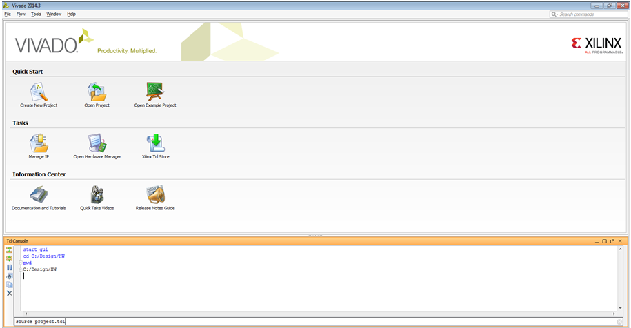 |
| Figure 1: Start of vivado project window |
Then after sourcing of project.tcl file the block diagram will open, like as shown below:
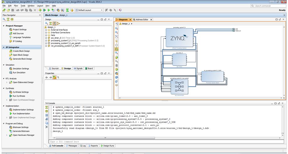 |
| Figure 2 : Block diagram view of AMP based DDR LESS Zynq system using AXI Timer in PL. |
2. In the Flow Navigator -> tab click on the Generate Bitstream
After the generation of bitstream, it opens an implemented design dialog box open, click on OK, and then implemented design opened as shown in figure 3 below:
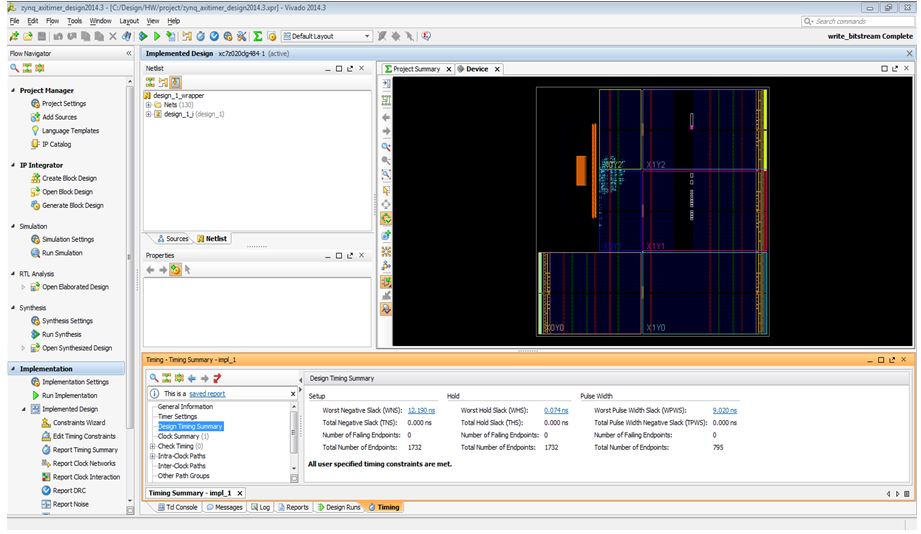 |
| Figure 3: Implemented Design view |
3. Then, Go to the File->Export-> click on Export hardware, The Export hardware diagram opens, then enable the Include bitstream and click ok.
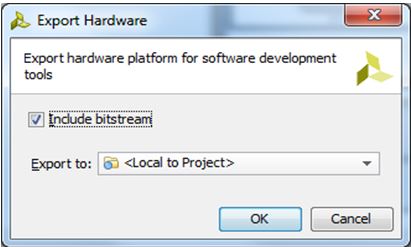 |
| Figure 4: Export hardware platform window. |
Next step is to export the hardware design to SDK.
4. For this go to the File-> click on Launch SDK.
The SDK window will be launched.
Software Implementation:
After SDK launch, the projects needs be to import.
- Select File->Import to open an import wizard.
- Select General > Existing Projects into Workspace in the import wizard.
- To select the root directory from which the projects need to be imported, click Browse and Specify the location >> where the software applications are stored. Assuming that the projects are downloaded at Windows C:\Design, for the software applications the >> windows location is C C:\Design\SW folder.
- The import wizard displays a list of projects that are available to import. This list should Include: fsbl_xip, fsbl_xip_bsp, design_1_wrapper_hw_platform_0, APP_CPU0 and APP_CPU1, APP_CPU1_bsp. Select all these projects to be imported. Select the option Copy projects into workspace, if you want local copies of these projects in the workspace. Finally select Finish.
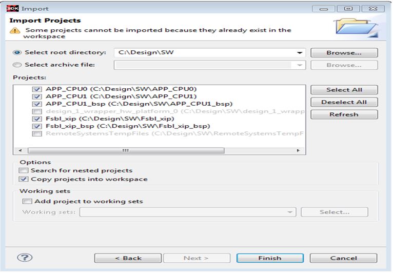 |
| Figure 5: Select Folder to Import Projects. |
Building programming file(mcs) for QSPI flash: A precompiled version of Application.mcs file is available at Design\generated_files\Application.mcs
All the files referred in this step are also precompiled and available at Design\genertated_files.
- Copy the included directory Design\bootgen to Design\<workspace>\bootgen. This directory includes the Bootgen batch file (createBoot.bat), a Boot image file (bootimage.bif).
- Generate mcs file using bootgen command.
- Modify the mcs file for XIP.
- Remove the intermediate files.
bootimage.bif file is configuration file which list the input files to the boot image along with optional attributes. It includes FSBL elf as a bootlaoder with offset 0x2000 and .bit file for PL and also APP_CPU0 elf with an offset 0x580000 and APP_CPU1 elf with an offset 0x700000, the attribute xip_mode which indicates the "Execute in Place". - Copy the compiled FSBL_xip ELF from
Design\<workspace>\<SDK_workspace>\FSBL_xip\Debug\FSBL_xip.elf into Design\work\bootgen
Note: If the steps were not taken to compile the FSBL in SDK, a copy is provided in the reference design at Design\generated_files\FSBL_xip.elf. - Copy the compiled Application0 (APP_CPU0) ELF from
Design\<workspace>\<SDK_Worspace>\APP_CPU0\Debug\APP_CPU0.elf into Design\work\bootgen
Note: If the steps were not taken to compile the FSBL in SDK, a copy is provided in the reference design at Design\generated_files\APP_CPU0.elf. - Copy the compiled Application1 (APP_CPU1) ELF from
Design\<workspace>\<SDK_Worspace>\APP_CPU1\Debug\APP_CPU1.elf into Design\work\bootgen
Note: If the steps were not taken to compile the FSBL in SDK, a copy is provided in the reference design at Design\generated_files\APP_CPU1.elf. - Open a Xilinx SDK Suite command prompt. This command prompt has the environment set up for the Xilinx tool.
- In the command prompt, change the directory to Design\work\bootgen.
- Run the createBoot.bat file. This creates the boot file Application.mcs in the current directory.
- QSPI Flash Programming Follow the following procedure to program QSPI flash
- Make sure that the hardware board is set up is done properly.
Note: Refer to UG873, Zynq-7000 SoC: Concepts, Tools, and Techniques, section2.1.3 TakeTestDrive!Runningthe“HelloWorld” Application for information about setting up the board. - Change the SW16 switch setting as shown below
- Make sure that the hardware board is set up is done properly.
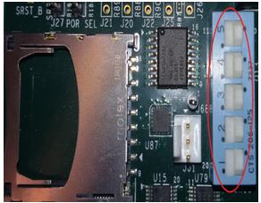 |
| Figure 6: Switch selections for SD boot. |
- In SDK, select Xilinx Tools > program flash.
It opens Program Flash Memory Wizard - In Image File tab, click Browse to navigate to Application.mcs file. Provide
Design\work\bootgen\Application.mcs - Select Verify after flash option.
- Click Program.
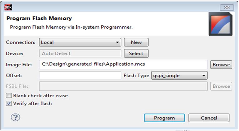 |
| Figure 7 : Select .mcs file for program flash memory. |
Application Execution From QSPI:
Follow the following procedure to execute application on the board
- After you program the QSPI Flash, set the SW16 switch on your board as shown in below figure.
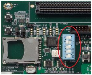 |
| Figure 8: Switch Selection for QSPI BOOT. |
- Open a serial communication utility for the com port
- Switch on the board power.
At startup, Bootcode, extract the residing address of FSBL from header and handover the execution to FSBL. FSBL executes and extract the residing address of Application from partition header information. Than it preload the application program data sections to the OCM memory. After that it handoff control to Application and start executing it. At the start of the execution application copies its own data section from Flash to OCM and at start sending prints on the serial terminal.
Monitor prints on the serial terminals. It displays information between two cores hello world.
Application Starts
CPU0: writing startaddress for cpu1
CPU0: sending the SEV to wake up CPU1
>>>>>>>>>> Hello World from CPU0 <<<<<<<<<
CPU1: init_platform
>>>>>>>> Hello World from : CPU 1 <<<<<<<<<<<
>>>>>>>>>> Hello World from CPU0 <<<<<<<<<<
>>>>>>>> Hello World from : CPU 1 <<<<<<<<<<<
Appendix A: File Descriptions in the design directory
Directory Structure is:
- Design
- HW
- Srcs: This folder has wrapper file (design_1_wrapper.v) for vivado project.
- Project.tcl: This .tcl file is used for sourcing vivado project.
- design_1.tcl: This .tcl file for block design of vivado project, this file will call in project.tcl file.
- SW:
- APP_CPU0: This Directory has core0 application and supporting files.
- APP_CPU1: This Directory has core1 application files.
- APP_CPU1_bsp: This folder has Supporting drivers for CPU1.
- Fsbl_xip: This Directory has bootloader source files.
- Fsbl_xip_bsp: This Directory has supporting driver files.
- design_1_wrapper_hw_platform_0: This directory has hardware project information.
- bootgen:
- bootimage.bif: This file has information regarding sequence of creating bootloader image.
- createBoot.bat: This file has bootgen command for creating .mcs file.
- generated_files:
- Application.mcs : mcs file for QSPI flash.
- Fsbl_xip.elf : FSBL executable.
- APP_CPU0.elf : Application executable for CPU0.
- APP_CPU1.elf : Application executable for CPU1.
- HW
Miscellaneous information:
- During the build of application projects we have got 3 errors namely:
APP_CPU1.elf: section `datasect' can't be allocated in segment 0
Fsbl_xip.elf: section `.data' can't be allocated in segment 0
These errors because of linker script modification in the memory section assignments.
These 3 linker script errors consider as a warnings, these errors not effect to build the projects.
© Copyright 2019 - 2022 Xilinx Inc. Privacy Policy