ZCU1275/ZCU1285 RFSoC 16X16 MTS Design Getting Started Guide
This 'Getting Started Guide' describes the components, features, and operation of the Xilinx® Zynq® UltraScale+™ RFSoC ZCU1275/ZCU1285 16x16 MTS Reference Design.
Table of Contents
Revision History
The following table shows the revision history of this document.
Date | Version | Revision | Comment |
|---|---|---|---|
| 2018.3 | 1.0 | ZCU1275 | |
| 2018.3.1 | 1.0 | ZCU1285 | |
| 2019.1 | 1.1 | ZCU1275/ZCU1285 | |
| 2019.2 | 1.2 | ZCU1275/ZCU1285 | |
| 2020.1 | 1.3 | ZCU1275/ZCU1285 | |
| 2020.1 | 1.4 | SMA-P to SMA-P Cable Length Correction | |
| 2020.2 | 1.5 | ZCU1275/ZCU1285 | |
| 2021.1 | 1.6 | ZCU1275/ZCU1285 |
Overview
The ZCU1275/ZCU1285 16x16 reference design demonstrates Multi-Tile Synchronization feature on RFSoC part. The design supports 16 DAC and 16 ADC channels. All the 16 DAC and 16 ADC channels are aligned.
The link for the design package is provided in ZCU1275/1285 16x16 MTS Package Download section.
The details about the design can be found in the following section MTS Design.
This tutorial contains information about:
- Procedure to setup the ZCU1275/ZCU1285 evaluation board and run this 16x16 MTS reference design.
- Procedure to build the design components based on the provided source files via detailed step-by-step tutorials.
This section provides the steps to build and run the ZCU1275/ZCU1285 16x16 MTS reference design. The design demonstrates the Multi-Tile Synchronization (MTS) feature of the RFdc (RF-ADC and RF-DAC) available in Zynq® UltraScale+™ RFSoC devices.
The ZCU1275/ZCU1285 16x16 MTS reference design is targeted to ZCU1275/ZCU1285 evaluation board. The ZCU1275/ZCU1285 16x16 reference design configures RF-ADCs & RF-DACs including the associated clocking system, to perform signal generation and capture using RFDACs & RFADCs and validate the MTS functionality.
Xilinx Vivado IPI flow is used to create the hardware design which is partitioned between the processing system (PS), RFDC IP, and programmable logic (PL). Xilinx PetaLinux flow is used to create and integrate the software components, including Linux kernel and drivers.
The system level block diagram of the 16x16 MTS reference design is shown in the below figure.
The ZCU1275/ZCU1285 16x16 MTS reference design runs on ZU29DR/ZU39DR RFSoC. The design has 16 independent DAC and ADC paths, two AXI DMAs and Stream Pipes components for high performance data transfers from PS_Memory to RFDC and vice versa. The Stream Pipes comprises of various AXI4 Stream Infrastructure IPs. The AXI DMA is configured in Scatter- Gather (SG) mode for high performance. The APU inside PS is configured to run in SMP Linux mode. The main task of the Linux application is to configure and control the RF-ADC& RF-DAC blocks and the flow of data through the streaming pipeline.
The design supports IQ mode of data. The data for the DAC is complex (IQ) with a phase difference of 90 degrees between I and Q data. The output of the DAC is loop backed to the ADC using SMA cables and DC blocking capacitors. The data received on the ADC is interleaved. The I and Q data are split and then plotted.
The ZCU1275/ZCU1285 16x16 reference design can be run in three separate modes:
- Standalone RF-DAC: - In this mode, a pattern is read from a SD card. The pattern is either sent once or constantly replayed on the selected RF-DAC channels based on the mode selected by a user. The output of the RF-DAC can be monitored on a standard external equipment like, Spectrum Analyzer or Oscilloscope.
- Standalone RF-ADC: - In this mode, an analog signal from an external equipment can be connected to the RF-ADC Inputs. The digital output of the RF-ADC can be analyzed by storing the received samples on SD card and plotting the wave forms using a Microsoft Excel application.
- RF-DAC to RF-ADC Loopback: - In this mode, the output of the RF-DAC is looped back to the input of RF-ADC using a BullsEye cables. A test pattern is read from a standard SD card and sent to the DAC channels. The received test pattern is stored back on the SD Card that can be verified by the wave forms using a Microsoft Excel application.
Requirements
Hardware
The following table shows the list of components that are obtained on purchasing the ZCU1275 kit.
Part number | Description | Quantity |
ZCU1275 | Char board with XCZU29DR-2FFVF1760I part | 1 |
HW-CLK-103 | SuperClock-RF2 module for RF clocks | 1 |
HW-CLK-101-SCLK2 | SuperClock-2 module for GT clocks | 1 |
MAXREFDES87# | Maxim MGT power modules (GTY and GTR) | 2 |
EVREF0102A | MPS Analog power module | 1 |
ISL8024 | Intersil Analog power module | 1 |
HW-SMA-RF100 | Balun Board | 1 |
AZCBL-USB-11002 | CABLE, USB 'A' MALE TO MICRO USB 'B' MALE, 6FT, ROHS | 2 |
RSP-200723-02-BEYE | Samtec Gen2 Bullseye cable | 2 |
AZCBL-SMA-18001 | Rosenberger SMA to SMA 12” cable | 2 |
VLFX-1300+ | Mini-Circuits DC-1300MHz filter | 2 |
VLFX-2500+ | Mini-Circuits DC-2500MHz filter | 2 |
8037 | Inmet DC block (for GTR loop back demo) | 2 |
132169 | Amphenol SMA to SMA adapter (for GTY loop back demo) | 16 |
132360 | Amphenol 50 ohm SMA termination | 8 |
PA1090-120T1A667-373-V0 | Digilent 12V power supply | 1 |
Power plug for US, EC, or UK | 1 | |
SDSDB-008G-B35 | Sandisk 8GB SD card | 1 |
The following table shows the list of components that are obtained on purchasing the ZCU1285 kit.
| Part Number | Description | Quantity |
|---|---|---|
ZCU1285 | Char board with XCZU39DR-2FFVF1760I part | 1 |
HW-CLK-103 | SuperClock-RF2 module for RF clocks | 1 |
HW-CLK-101-SCLK2 | SuperClock-2 module for GT clocks | 1 |
MAXREFDES87# | Maxim MGT power modules (GTY and GTR) | 2 |
EVREF0102A | MPS Analog power module | 1 |
ISL8024 | Intersil Analog power module | 1 |
HW-SMA-RF200 | Balun Board | 1 |
AZCBL-USB-11002 | CABLE, USB 'A' MALE TO MICRO USB 'B' MALE, 6FT, ROHS | 2 |
RSP-200723-02-BEYE | Samtec Gen2 Bullseye cable | 2 |
AZCBL-SMA-18001 | Rosenberger SMA to SMA 12” cable | 2 |
VBFZ-3590+ | DOCSIS 3000-4300MHz filter | 2 |
VLFX-2500+ | Mini-Circuits DC-2500MHz filter | 2 |
| ZX75PP-4700-S+ | Mini-Circuits 4400-5000MHz filter | 2 |
8037 | Inmet DC block (for GTR loop back demo) | 2 |
132169 | Amphenol SMA to SMA adapter (for GTY loop back demo) | 16 |
132360 | Amphenol 50 ohm SMA termination | 8 |
PA1090-120T1A667-373-V0 | Digilent 12V power supply | 1 |
Power plug for US, EC, or UK | 1 | |
SDSDB-008G-B35 | Sandisk 8GB SD card | 1 |
Design Tools and Software
- Vivado Design Suite(2018.3 onwards)
- Linux host machine for all tool flow tutorials (see UG1144 for detailed OS requirements).
- PetaLinux Tools (see UG1144 for installation instructions).
- Git distributed version control system.
- Silicon Labs quad CP210x USB-UART bridge driver
- Serial terminal emulator e.g. teraterm
- Reference Design Zip File.
Download, Installation and Licensing
The Vivado Design Suite User Guide explains how to download and install the Vivado® Design Suite tools, it includes the Vivado Integrated Design Environment (IDE), High Level Synthesis tool. This guide also provides the information about licensing and administering evaluation and full copies of Xilinx design tools and intellectual property (IP) products. The Vivado Design Suite can be downloaded from here.
ZCU1275/1285 16x16 MTS Package Download
The package files to demonstrate the MTS features can be downloaded from the following pages at Xilinx.com:
Design Files
The top-level directory structure shows the major design components organized as shown below. A Pre-Built SD card image (BOOT.BIN and image.ub) is provided along with a basic README and legal notice file.
Procedure to program system controller on ZCU1275/ZCU1285 Evaluation Board
The ZCU1275/ZCU1285 board uses a Xilinx XC7Z010-CLG225 Zynq-7000 SoC System Controller U38 that can be used to configure the output frequencies of the Clock Module.
Please update the Zynq-7000 firmware that configures the clock module as listed under "Programming Instruction Steps"
Requirements
- Platform Cable USB or Platform Cable USB II
- Micro USB cable
- Vivado 2014.1 or later
- The procedure described below is not compatible with Vivado 2013.4 or earlier
- ZIP file (qspi_image_rev10.zip) containing the .mcs file (The zip file is provided in the design package at " ../hw-clk-102 " folder)
- ZIP file (SD_card_clocks) (The zip file is provided in the design package at " ../hw-clk-102 " folder)
Programming Instruction Step for hw-clk-102
The HW-CLK-102 has 2 PLL's, PLL A and PLL B. 8 clocks are needed (4 for each DAC and ADC tile) to validate the complete 16x16 MTS design. The HW-CLK-102 has only 6 clock sources (4 in PLL A and 2 in PLL B) totally and hence is not sufficient to provide clocks for all the DAC's and ADC's.
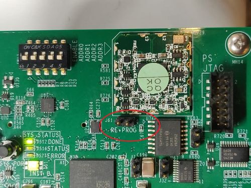
- Place a shunt on J61 (RE_PROG) prior to power up the ZCU1275/ZCU1285.
- Extract the .mcs file from the ZIP (qspi_image_rev10.zip) file to a working directory. This is provided in the design package at " ../hw-clk-102 " folder.
- Close any active JTAG cable communication sessions with Platform Cable USB or the Digilent USB-JTAG module.
- Disconnect the Serial Port in TeraTerm if applicable (File->Disconnect).
- Power off the ZCU1275/ZCU1285 board.
- If it is connected, remove the JTAG ribbon cable between Platform Cable USB and J2.
- If it is connected, remove the micro USB cable from the Digilent USB-JTAG module.
- Connect the JTAG ribbon cable between Platform Cable USB and connector J3 on ZCU1275/ZCU1285.
- Power on the ZCU1275/ZCU1285 board.
- Start Vivado.
- In Vivado, open Hardware Manager.
- When Hardware Manager appears, click on Open a new hardware target.
- When the Open New Hardware Target dialog box appears, click Next and then Next again.
- When prompted to Select Hardware Target, click Next and then Finish.
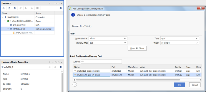
- In the Hardware panel of the Vivado GUI, right click zc7z010_1and select Add Configuration Memory Device (see figure to the right).
- When the Add Configuration Memory Device dialog box appears, find and select memory part n25q128-qspi-x4-single(Caution: do not confuse n25q128 with n25q128a. If 3.3V and 1.8V devices listed separately, select n25q128-1.8v-qspi-x4-single) then click OK.
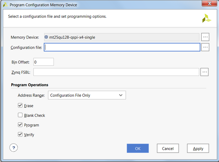
17. When prompted to “Select a configuration file and set programming options”.
- Click on the button to the right of the Configuration file field and navigate to the "XIP_Application.mcs" file extracted in step 2.
- Click on the button to the right of the Zynq FSBL field and navigate to the "zynq_1b_debug_fsbl.elf" file extracted in step 2.
- Confirm that there are checks next to Erase, Program and Verify.
18. Before starting programming, remove the shunt on J61(Re_PROG). DO NOT skip this step.
19. Finally, click OK to start the programming of the QSPI memory device.
20. Remove Xilinx USB-II JTAG cable from J3.
21. Unzip the “SD_card_Clocks” folder and load the SD Card with the clock configuration boot files provided in this folder
as shown in the figure below.
The zip file are provided in the design package at " ../hw-clk-102 " folder.
22. Insert the pre-loaded SD card prior to power cycle ZCU1275/ZCU1285.
23. Install HW-CLK-102 on J170 and Analog power module on J131,J119 and J120 of ZCU1275.
24. Confirm one shunt on J125 @I2C location of ZCU1275/ZCU1285.
25. Plug in the USB cable on J1 of ZCU1275/ZCU1285 and power cycle it.
26. All the 4 LEDs on CLK-102 module should be lighting up after power-up.
Programming Instruction Step for hw-clk-103
The HW-CLK-103 has 3 PLL's, PLL A ,PLL B and PLL C. 8 clocks are needed (4 for each DAC and ADC tile) to validate the complete 16x16 MTS design. The HW-CLK-103 has 8 clock sources (4 in PLL A, 2 each in PLL B and PLL C) totally and is sufficient to provide clocks for all the DAC's and ADC's.
- The System Controller User Interface (SCUI) package for ZCU1275/ZCU1285 can be downloaded from here.
- Extract the package and follow the steps in readme file to program system controller firmware on to the board.
Unzip the "clockFiles" zip folder in the hw-clk-103 section from the design package. Replace the clock Files folder in the ZCU1275/ZCU1285 SCUI package with the clock Files from the design package.
- Install HW-CLK-103 on J170.
- The procedure to program the clocks on HW_CLK_103 can be found on Clock Configuration Using System Controller User Interface (SCUI).
Board Setup
Jumpers and Switches
The Board can be set up by following the steps given below.
Refer to the “ZCU1285 Characterization Board User Guide” UG1285 for default jumper and switch settings.
The following jumpers and switches need to be changed or need to be confirmed to be in the following states for this design.
The following steps are helpful while setting up the board.
- Make sure the J61 jumper (RE-PROG) is removed on ZCU1275/ZCU1285.
2. Confirm J37 Jumper is placed for UART Enable and J103 for QSPI Enable (Close)
3. Connect UART cable to J1 connector on ZCU1275/ZCU1285.
4. Confirm the Jumpers J163, J164, J165 and J166 are connected in SD Card Boot Mode for RFSoC as shown in below figure.
5. Please make sure that Analog Power Module is place on J131, J119 and J120.
6. HW-CLK-103 daughter card is necessary to access analog and clock port for RF Data Converters. Please connect the Clock Module HW-CLK-103 to the clock module interface connector of ZCU1275/ZCU1285.
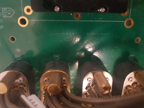
7. Connect Bulls Eye Cables to J129 of ZCU1275/ZCU1285 for DAC connections and to J124 of ZCU1275/ZCU1285 for ADC connections.
8. The figure below shows the layout of the Bulls-Eye connectors.
- Connect the pin VOUT0 of DAC to pin VIN_0 of ADC (positive terminals). Do not forget to connect the DC blocking capacitor
- Connect the pin VOUT0 of DAC to pin VIN_0 of ADC (negative terminals). Do not forget to connect the DC blocking capacitor
Similarly, make connections for the rest of the DACs and ADCs.
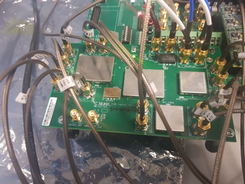
Connecting Clocks between ZCU1275/ZCU1285 board and Clock Module(HW-CLK-103) for DAC Analog Clocks, ADC Analog Clocks, PL REF CLK, PL SYSREF and SYSREF CLK:
DAC Analog Clocks
DAC Tile 0 clock_P : Connect Cable 9 of ZCU1275/ZCU1285 Bulls Eye interface (J129) to the RF_CLK0_A1_P(J12) of Clock Module(HW-CLK-103)
DAC Tile 0 clock_N : Connect Cable 10 of ZCU1275/ZCU285 Bulls Eye interface (J129) to the RF_CLK0_A1_N(J13) of Clock Module(HW-CLK-103)
DAC Tile 1 clock_P : Connect Cable 12 of ZCU1275/ZCU1285 Bulls Eye interface (J129) to the RF_CLK0_A2_P(J14) of Clock Module(HW-CLK-103)
DAC Tile 1 clock_N : Connect Cable 11 of ZCU1275/ZCU1285 Bulls Eye interface (J129) to the RF_CLK0_A2_N(J15) of Clock Module(HW-CLK-103)
DAC Tile 2 clock_P : Connect Cable 9 of ZCU1275/ZCU1285 Bulls Eye interface (J279) to the RF_CLK0_A3_P(J16) of Clock Module(HW-CLK-103)
DAC Tile 2 clock_N : Connect Cable 10 of ZCU1275/ZCU1285 Bulls Eye interface (J279) to the RF_CLK0_A3_N(J17) of Clock Module(HW-CLK-103)
DAC Tile 3 clock_P : Connect Cable 12 of ZCU1275/ZCU1285 Bulls Eye interface (J279) to the RF_CLK0_A4_P(J18) of Clock Module(HW-CLK-103)
DAC Tile 3 clock_N : Connect Cable 11 of ZCU1275/ZCU1285 Bulls Eye interface (J279) to the RF_CLK0_A4_N(J19) of Clock Module(HW-CLK-103)
ADC Analog Clocks
ADC Tile 0 clock_P : Connect Cable 9 of ZCU1275/ZC1U285 Bulls Eye interface(J124) to the RF_CLK0_B1_P(J20) of Clock Module(HW-CLK-103)
ADC Tile 0 clock_N : Connect Cable 10 of ZCU1275/ZCU1285 Bulls Eye interface(J124) to the RF_CLK0_B1_N(J21) of Clock Module(HW-CLK-103)
ADC Tile 1 clock_P : Connect Cable 12 of ZCU1275/ZCU1285 Bulls Eye interface(J124) to the RF_CLK0_B2_P(J23) of Clock Module(HW-CLK-103)
ADC Tile 1 clock_N : Connect Cable 11 of ZCU1275/ZCU1285 Bulls Eye interface(J124) to the RF_CLK0_B2_N(J22) of Clock Module(HW-CLK-103)
ADC Tile 2 clock_P : Connect Cable 9 of ZCU1275/ZCU1285 Bulls Eye interface(J278) to the RF_CLK0_C1_P(J26) of Clock Module(HW-CLK-103)
ADC Tile 2 clock_N : Connect Cable 10 of ZCU1275/ZCU1285 Bulls Eye interface(J278) to the RF_CLK0_C1_N(J29) of Clock Module(HW-CLK-103)
ADC Tile 3 clock_P : Connect Cable 12 of ZCU1275/ZCU1285 Bulls Eye interface(J278) to the RF_CLK0_C2_P(J27) of Clock Module(HW-CLK-103)
ADC Tile 3 clock_N : Connect Cable 11 of ZCU1275/ZCU1285 Bulls Eye interface(J278) to the RF_CLK0_C2_N(J28) of Clock Module(HW-CLK-103)
PL REF CLK
Connect J84(CLK_DIFF_1 P) of ZCU1275/ZCU1285 to J4(FPGA REF CLK P) of Clock Module(HW-CLK-103) for PL REF CLK connection
Connect J85(CLK_DIFF_1 N) of ZCU1275/ZCU1285 to J5(FPGA REF CLK N) of Clock Module(HW-CLK-103) for PL REF CLK connection
PL SYSREF
Connect J83(CLK_DIFF_2 P) of ZCU1275/ZCU1285 to J8(SYS_REF_2_P) of Clock Module(HW-CLK-103) for PL SYSREF CLK connection
Connect J86(CLK_DIFF_2 N) of ZCU1275/ZCU1285 to J9(SYS_REF_2_N) of Clock Module(HW-CLK-103) for PL SYSREF CLK connection
SYSREF
Connect J242(SYSREF_228_P) of ZCU1275/ZCU1285 to J6(SYS_REF_1_P) of Clock Module(HW-CLK-103) for SYSREF CLK connection
Connect J243(SYSREF_228_N) of ZCU1275/ZCU1285 to J7(SYS_REF_1_N) of Clock Module(HW-CLK-103) for SYSREF CLK connection
- Connect J1 to your host PC via USB cable and plug in power connector (J28). Connect the power adapter to AC power.
- Prepare the Micro SD card (See Micro SD Card Preparation section for more details)
- Set up a Tera Term session between a host PC COM port and the serial port on the evaluation board (See How to Identify the COM Port section for more details).
Micro SD Card Preparation
The Micro SD Card can be prepared in the following manner.
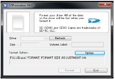
- Prepare the Micro SD card. Use SD formatter tool to create a FAT partition,https://www.sdcard.org/downloads/formatter_4/
2. Copy all the files from the $TRD_HOME/images/rev-B to FAT formatted SD card.
How to Identify the COM Port
Make sure that the ZCU1275/ZCU1285 board is powered on and a micro USB cable is connected between ZCU1275/ZCU1285 board (Micro USB Port) and host PC. This ensures that the USB-to-serial bridge is enumerated by the host PC.
- Open your computer's Control Panel by clicking the Start > Control Panel. Note that the Start button is typically located in the lower left corner of the screen. Occasionally, it is in the upper left corner.
- Click the Device Manager to open the Device Manager window. Note that you may be asked to confirm opening the Device Manager. If so, click YES.
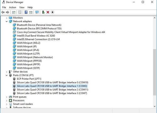
- Expand Ports (COM & LPT). You will see four USB Serial Port (COM#).
- In the below figures Interface1(COM#) should be used for clock configuration of HW-CLK-103 clock module. Interface2(COM#) should be used for serial logs and to run "rfdcmtstest" application.
Above information mentioned in diagram is applicable for windows 10/windows 7 operating System only.
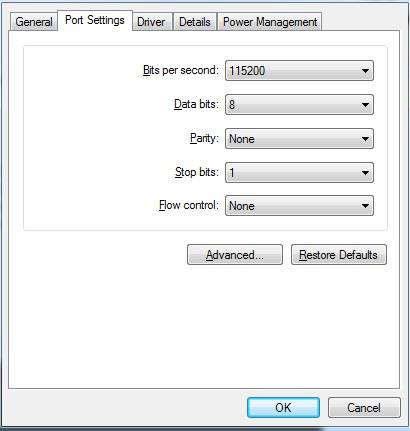
5. In the properties window, select the Port Settings Tab. Set Bits per second,Data bits,Parity,Stop bits, and Flow control to the values shown in the below figure, and click OK.
6. Note down the COM Port number for further steps.
RFSoC RFdc Build and Run Flow Tutorial
The following link will navigate the reader to ZCU1275/ZCU1285 MTS Design Example page.
Performance Metrics
The performance metrics of the designs can be verified here.
Support
To obtain technical support for this reference design, go to the:
- Xilinx Answers Database to locate answers to known issues.
- Xilinx Community Forums to ask questions or discuss technical details and issues. Please make sure to browse the existing topics first before filing a new topic. If you do file a new topic, make sure it is filed in the sub-forum that best describes your issue or question e.g. Embedded Linux for any Linux related questions. Please include "ZCU1275/ZCU1285 RFSoC TRD" and the release version in the topic name along with a summary of the issue.
Child Pages
© Copyright 2019 - 2022 Xilinx Inc. Privacy Policy
