ZCU111 RFSoC RF Data Converter Evaluation Tool Getting Started Guide
Table of Contents
In the 2018.2 version of the design, all the features were the part of a single monolithic design. In the subsequent versions the design has been split into three designs based on the functionality.
Revision History
The following table shows the revision history of this document.
Date | Version | Revision |
|---|---|---|
| 2018.2 | Alpha-1.0 |
| 2018.2 | Beta-1.0 |
| 2018.2 | 1.0 |
| 2018.3 | 1.3 | |
| 2019.1 | 1.4 | |
| 2019.2 | 1.5 | |
| 2020.1 | 1.6 | |
| 2020.2 | 1.7 | |
| 2021.1 | 1.8 |
Feature Matrix Table
The Matrix table for various features are given below.
| Feature | SSR IP (1X1) | Non-MTS (8X8) | MTS (8X8) |
|---|---|---|---|
| 8X8 | NO | YES | YES |
| BRAM Mode | YES | YES | YES |
| DDR Mode | YES | YES | NO |
| Real/Complex | Real Only | Both Real & IQ | Real Only |
| QMC | NO | YES | NO |
| Multiband | NO | YES | NO |
| SSR | YES | NO | NO |
| Power Advantage Tool | NO | YES | NO |
| Interpolation/Decimation | YES | YES | NO |
| Mixer | NO | YES | NO |
| 20/32 mA | YES | YES | YES |
| Internal PLL | YES | YES | NO |
| ADC Calibration | YES | YES | YES |
| Nyquist | YES | YES | NO |
| High Linearity/Low Noise | YES | YES | NO |
| Inverse Sync Filter | YES | YES | NO |
Overview
As mentioned above,in the 2018.2 version of the design, all the features were the part of a single monolithic design. In the subsequent versions the design has been split into three designs based on the functionality. A detailed information about the three designs can be found from the following pages.
This tutorial contains information about:
- How to setup the ZCU111 evaluation board and run the Evaluation Tool.
- How to build all the Evaluation Tool components based on the provided source files via detailed step-by-step tutorials.
- Performance Numbers
Additional material not covered in this tutorial
- Zynq UltraScale+ ZCU111 RFSoC RF Data Converter TRD user guide, UG1287
- The UG provides the list of device features, software architecture and hardware architecture.
This document provides the steps to build and run the RFSoC RF Data Converter Evaluation Tool. The design demonstrates the capabilities and performance of the RFdc (RF-ADC and RF-DAC) available in Zynq® UltraScale+™ RFSoC devices. The Evaluation Tool serves as a platform for Xilinx customers to evaluate the Zynq® UltraScale+™ RFSoC features and helps them to accelerate the product design cycle.
The Evaluation Tool consists of a ZCU111 evaluation board and a custom graphical user interface (UI) installed on a Windows host machine. The Evaluation Tool allows user to configure the operation of the RF-ADCs & RF-DACs including the associated clocking system, to perform signal generation and capture using RFDACs & RFADCs and to perform RF metrics computation on signal capture for input test signals.
Xilinx Vivado IPI flow is used to create the hardware design which is partitioned between the processing system (PS), RFDC IP, and programmable logic (PL). Xilinx PetaLinux flow is used to create and integrate the software components, including Linux kernel and drivers.
The system level block diagram of the Evaluation Tool design is shown in the below figure.
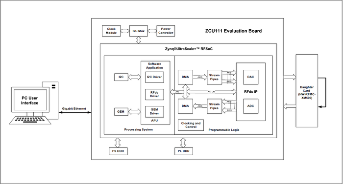 The Evaluation Tool uses an integrated ZU28DR RFSoC which is of 8x8 configuration along with AXI DMA and Stream Pipes components for high performance data transfers from PL-DDR to RFDC and vice versa. The Stream Pipes comprises of various AXI4 Stream Infrastructure IPs. The AXI DMA is configured in Scatter- Gather (SG) mode for high performance. The Evaluation Tool also makes use of multiple processing units available inside the PS like Gigabit Ethernet, I2C, and SD Interface. The APU inside PS is configured to run in SMP Linux mode. The main task of the Linux application is to configure and control the RF-ADC& RF-DAC blocks and the flow of data through the streaming pipeline.
A custom developed Windows-based user interface (UI) is provided along with the Evaluation Tool. It can interact with the RFSoC device running on the ZCU111 evaluation board. The UI connects to the Linux application running on RFSoC via a TCP Ethernet interface. Based on the commands received from the UI on the host machine, the Linux application on the RFSoC device performs various operations that are described later in the user guide. As a TCP socket is used to transfer the data over Ethernet, it is possible to run the UI on any machine connected to the network.
The Evaluation Tool can be run in three separate modes:
- Standalone RF-DAC: - In this mode, a pattern can be generated using the UI on the host machine. This pattern is constantly replayed on the selected RF-DAC channel. The output of the RF-DAC can be monitored on a standard external equipment like, Spectrum Analyzer or Oscilloscope.
- Standalone RF-ADC: - In this mode, an analog signal from an external equipment can be connected to the RF-ADC Inputs. The digital output of the RF-ADC can be analyzed on the host machine using UI.
- RF-DAC to RF-ADC Loopback: - In this mode, the output of the RF-DAC is looped back to the input of RF-ADC using a daughter card (HW-RFMC-XM500) and SMA cables. A test pattern is generated on the host PC using UI and is sent to the RFSoC by the Ethernet interface. The received test pattern is stored into PL-DDR memory. The stored pattern is then sent to RF-DAC using AXI DMA and Stream Pipe for conversion to analog signal. The transmitted analog signal is looped back into the RF-ADC for converting the analog signal into a digital signal. Once digitized, it is stored into PL-DDR memory using AXI DMA and Stream Pipe and is sent back to the host by the Ethernet interface for analysis.
Requirements
Hardware
- ZCU111 evaluation board with the Zynq® UltraScale+™ RFSoC ZU28DR-FFVG1517 device
- Power Supply: 100 VAC–240 VAC input, 12 VDC 5.0A output
- One USB cable, standard-A plug to micro-B plug
- One Ethernet cable
- One daughter card (HW-RFMC-XM500)
- SMA cables
- Class-10 Micro SD card
- Cables and Filters Supplied with the board
Design Tools and Software
- Vivado Design Suite (2018.3 onwards)
- Linux host machine for all tool flow tutorials (see UG1144 for detailed OS requirements)
- PetaLinux Tools (see UG1144 for installation instructions)
- Git distributed version control system
- FTDI USB-UART bridge driver
- Serial terminal emulator e.g. teraterm
- Reference Design Zip File
- RF_DC_Evaluation_UI.exe - UI executable installed on Windows 7/10 Machine
Download, Installation and Licensing
The Vivado Design Suite User Guide explains how to download and install the Vivado® Design Suite tools, it includes the Vivado Integrated Design Environment (IDE), High Level Synthesis tool, and System Generator for DSP. This guide also provides the information about licensing and administering evaluation and full copies of Xilinx design tools and intellectual property (IP) products. The Vivado Design Suite can be downloaded from here.
The Evaluation Tool Package can be downloaded from the links below. The user needs to login and provide the necessary details to download the package.
ZCU111 Package Locations
Note: Please refer to this Answer Record for Known issues and limitations related to current version of RFSoC Evaluation tool release.
Design Files
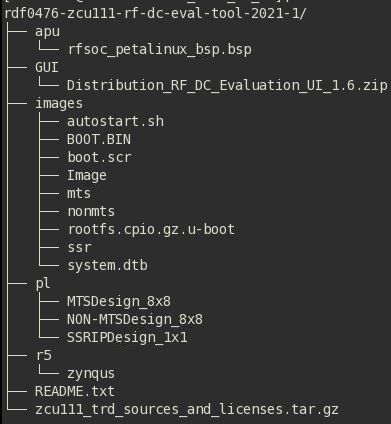
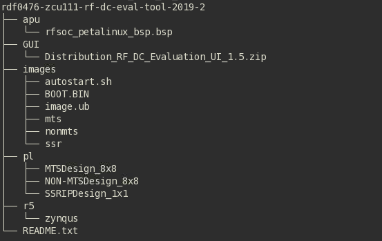
The top-level directory structure shows the major design components organized is shown below. A Pre-Built SD card image (BOOT.BIN and image.ub) is provided along with a basic README and legal notice file.
2018.3
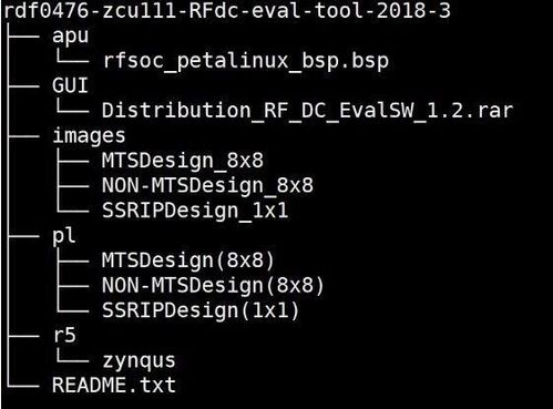
2019.1
2019.2
2020.1
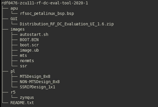
2021.1
2021.2
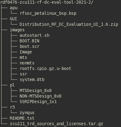
Board Setup
Board Connections
1. There are many jumpers and switches on the board, shipped with default states, which do not need to change for this Evaluation Tool design to work (See ZCU111 Jumper Settings for default jumper and switch settings).
2. XM500 daughter card is necessary to access analog and clock port of converters. Refer to below figure. Insert XM500 into J47 and J94 and secure it with screws.
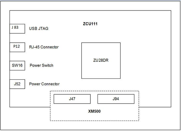
3. Connect J83 to your host PC via USB cable, connect P12 to host PC via Ethernet cable, and plug in power connector (J52). Connect the power adapter to AC power.
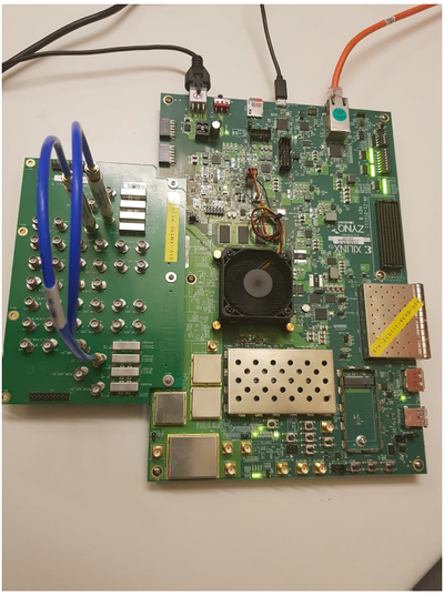
Once the above steps are followed, the board setup is as shown in the following figure:
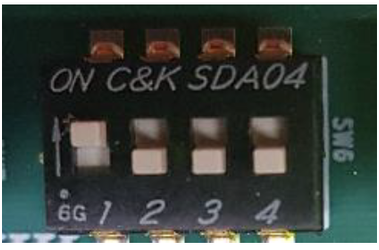
4. Make sure the DIP switches (SW6) are set as shown in the figure below, which allows the ZCU111 board to boot from the SD card.
5. Insert Micro SD Card into the user machine. To prepare the Micro SD card See Micro SD Card Preparation.
6. Set up a Tera Term session between a host PC COM port and the serial port on the evaluation board (See How to Identify the Comp Port section for more details).
7. User needs to set Ethernet IP Address for both Board and Host (Windows PC).
8. To Set Board Ethernet IP Address, Modify Autostart.sh (part of Images Folder in package). By Default, Board IP is configured to 192.168.1.3 in Autostart.sh file.
9. On Windows host PC, open RF_DC_Evaluation_UI.ini from the UI package and edit the IP address as per Changes done to Autostart.sh to match Board IP Address. This way UI will discover Board IP Address.
10. User needs to assign a static IP address in the host machine. Follow the instructions provided here.
Example:
IP address: 192.168.1.2
Subnet mask: 255.255.255.0
Default gateway: 192.168.1.1
Note: Please make sure
- The last digit of the IP Address on host should be different than what is being set on the Board.
- The default gateway should have last digit as one, rest should be same as IP Address field.
- Refer to the snapshot below for IP Setting in all 3 places.
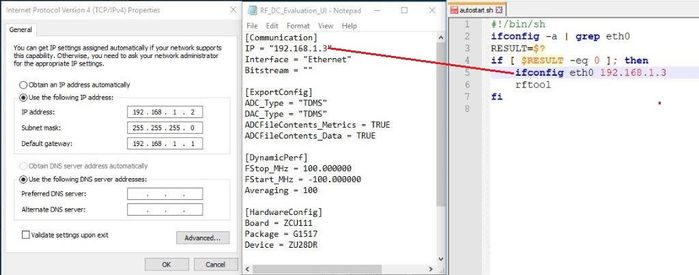
NOTE: As shown in the snapshot above
a. Left window explains about IP address setting on the host machine.
b. Middle Window explains IP address setting in .INI file of UI.
c. Right corner window explains IP address setting in autostart.sh present in SD card (which is IP address of the board).
11. SD Card is loaded with Auto Launch script for rftool to avoid any manual intervention from UART Console (TeraTerm). On UART Console the boot message will start as shown in figure below, no user intervention is required here it is only for sanity purpose.

NOTE: - SD Card Auto Launch Script should have same IP address as configured in UI’s .INI File
12. To Install the UI refer the UI Installation Section.
13. Launch the UI by running "RF_DC_Evaluation_UI.exe" executable.
Micro SD Card Preparation
Prepare the Micro SD card. Use SD formatter tool to create a FAT partition,https://www.sdcard.org/downloads/formatter_4/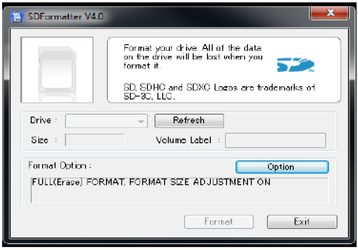
Copy all the files to FAT formatted SD card.
How to Identify the COM Port
Make sure that the ZCU111 board is powered on and a micro USB cable is connected between ZCU111 board (Micro USB Port) and host PC. This ensures that the USB-to-serial bridge is enumerated by the host PC.
1. Open your computer's Control Panel by clicking the Start > Control Panel. Note that the Start button is typically located in the lower left corner of the screen. Occasionally, it is in the upper left corner.
2. Click the Device Manager to open the Device Manager window. Note that you may be asked to confirm opening the Device Manager. If so, click YES.
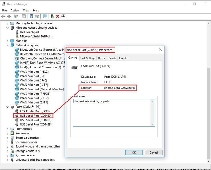
3. Expand Ports (COM & LPT). You will see three USB Serial Port (COM#).ZCU111 evaluation board uses FTDI USB Serial Converter B device.
4. Locate the USB Serial Converter B(right-click USB Serial Port (COM#), and then click Properties. Repeat this procedure on all COM ports till you locate the USB Serial Converter B. See below figure).
NOTE: Above information mentioned in diagram is applicable for windows 10/windows 7 operating System only.
5. In the properties window, select the Port SettingsTab. Set Bits per second,Data bits,Parity,Stop bits, and Flow control to the values shown in the below figure, and click OK.
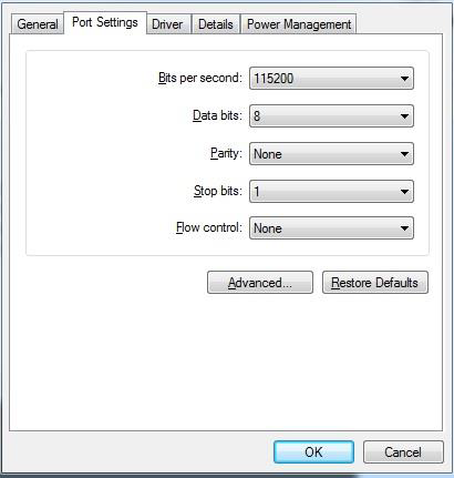
6.Note down the COM Port number for further steps.
UI Installation
The Zip for UI contains an Installer which will install all the components of UI and its associated software libraries. Please refer Design Files section for the folder structure of the package.
1) Extract All the Zip contains into a folder.
2) Browse through the Distribution_RF_DC_EvalSW_1.3 Folder and Double click on the Setup_RF_DC_Evaluation_UI_1.2.
3) Select the install path and click Next
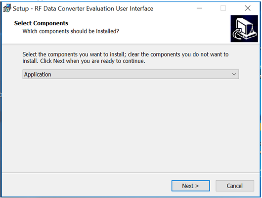
4) Select the Application and Click Next
5) Click on Install for complete installation
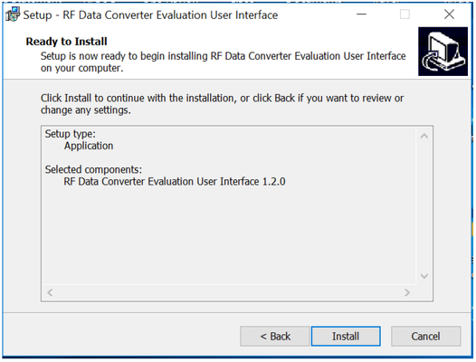
6) GUI will be auto launched after installation.
RFSoC RFdc Build and Run Flow Tutorial
The following link will navigate the reader to Zynq UltraScale+ RFSoC Data Converter Evalution Tool page.
Power Advantage Tool (PAT)
The Power Advantage Tool is a demo designed to showcase the power features of the Zynq UltraScale+ MPSoC device. For More details about PAT click on the link below.
Note: PAT feature works only with Non-MTS Design. Power Advantage Tool.
Test Setup
Figure below shows the loopback test setup.
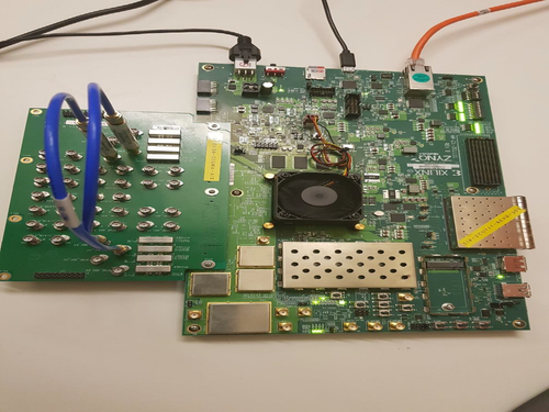
Note:The Evaluation Tool design supports 8x8 channels within limitations as described in Appendix A Performance Table.
RFdc Example Program
The Evaluation tool consists of 3 example programs which can be executed in a standalone manner i.e. without using UI configuration. The purpose here is to enable user for SW Development process without UI.
Note: The Example Programs are applicable only for Non-MTS Design.
Example Program 1
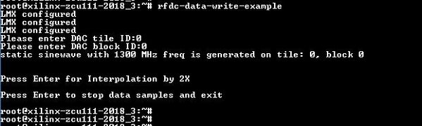
This application generates a sine wave on DAC channel selected by user. The user must connect the channel outputs to CRO to observe the sine waves. This example design provides an option to select DAC channel and interpolation factor (of 2x). By default, the application generates a static sinewave of 1300MHz.
The detailed application execution flow is described below:
1. Configure LMK with frequency to 122.88 MHz(REVAB). Refer the below table for frequency and offset values.
Board Version | Board Offset | Frequency |
|---|---|---|
REVA | 0 | 122.88 MHz |
REVAB | 1 | 122.88 MHz |
REVB | 2 | 122.88 MHz |
2. Configure LMX frequency to 245.76 MHz (offset: 2).
3. Configure Internal PLL for specified frequency. (3932.16 MHz).
4. Select DAC channel (by entering tile ID and block ID).
5. Get DAC memory pointer for the corresponding DAC channel.
6. Copy static sine wave pattern to target memory.
7. Disable "Channel X Control" GPIO (X = 0…7) for corresponding DAC.
8. Select requested DAC channel by configuring "streaming MUX" GPIO/scratch pad register.
9. Assert External "FIFO RESET" for corresponding DAC channel.
10. De-assert External "FIFO RESET" for corresponding DAC channel.
11. Enable RFDC FIFO for corresponding DAC channel.
12. Trigger DMA for selected DAC.
13. On DMA completion, enable "loopback GPIO " and "Channel X Control" GPIO (X = 0…7) as per selected DAC.
14. Wait for the user input.
15. Disable RFDC FIFO.
16. Set RFdc clock division factor by 2.
17. Set RFdc interpolation factor by 2.
18. Enable RFDC FIFO.
NOTE: Before running the examples, user must ensure that rftool application is not running.
To run this example, enter the following command at the console:
# rfdc-data-write-example
Below snapshot depicts response for the above command.
Example Program 2
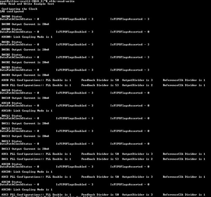
The Read/Write example design will wait until the RF-ADC/DAC block has initialized per the initial Vivado ADC/DAC setup, read that initial setup using API calls, then copying those setup parameters start an additional ADC and DAC block, then declare a pass/fail. Also printing out the written parameters along with the new ADC and DAC tile and block locations. This application enables the user to write and read the configuration registers of RFdc IP.
Note: This program is part of RFDC Software Driver code itself.
To run this example, enter the following command at the console:
# rfdc-read-write
Below snapshot depicts response for the above command.
Example Program 3
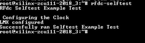
The Selftest example design will wait until the RF-ADC/DAC block has initialized per the initial ADC/DAC Vivado setup, then using API calls, check all the executable parameters of the RF-ADC/DAC block against the expected setup, compare those, and declare a pass/fail. Also printing out the expected vs. read parameters. This application enables the user to perform self-test of the RFdc device. It performs the sanity checks and restore the original settings after reset.
Note: This program is part of RFDC Software Driver code itself.
To run this example, enter the following command at the console:
# rfdc-selftest
Below snapshot depicts response for the above command.
NOTE: After running example applications, user need to either power cycle the board or run rftool application before launching the GUI.
Steps to compile R5 Hello World application
If SDK is used to create R5 hello world application using the shared XSA . User needs to select "libmetal" library (as shown in figure below) as RFSoC drivers are dependent on libmetal. Otherwise it will lead to compilation errors.

ZCU111 Jumper and Switch Settings
Figure below shows the ZCU111 board jumper header and switch locations. Each numbered component shown in the figure is keyed to Tables.
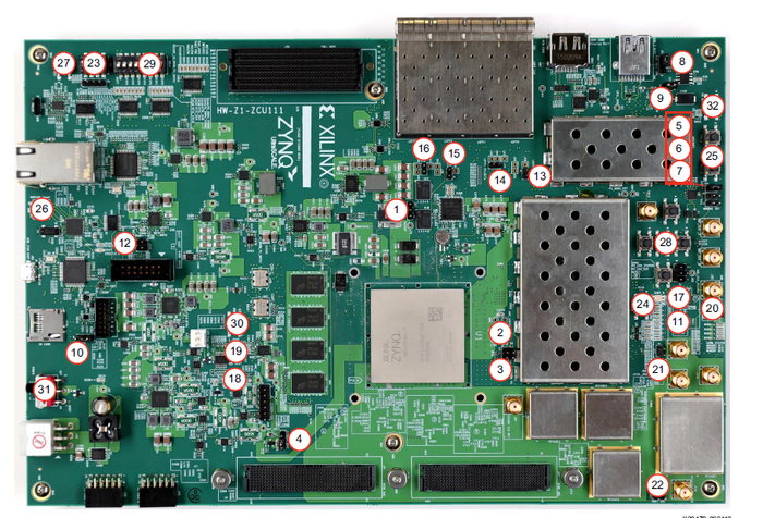
Jumpers
Callout Number | Ref Des | Function | Default |
|---|---|---|---|
1 | J85 | POR_OVERRIDE | 2-3 |
1-2: Enable | |||
2-3: Disable | |||
2 | J2 | SYSMON I2C address | On |
Off: SYSMON_VP_R floating | |||
On: SYSMON_VP_P pulled down | |||
3 | J3 | SYSMON I2C Address | On |
Off: SYSMON_VN_R floating | |||
On: SYSMON_VP_N pulled down | |||
| 4 | J4 | SYSMON VREFP | 1-2 |
| 1-2: 1.25V VREFP connected to fpga | |||
| 2-3: VREFP connected to GND | |||
| 5 | J20 | Reset sequencer PS_POR_B | On |
| Off: sequencer does not control PS_POR_B | |||
| On: sequencer can control PS_POR_B | |||
| 6 | J8 | Reset sequencer PS_SRST_B | On |
| Off: sequencer does not control PS_SRST_B | |||
| On: sequencer can control PS_SRST_B | |||
| 7 | J9 | Reset sequencer inhibit | Off |
| Off: sequencer normal operation | |||
| On: sequencer inhibit (resets will stay asserted) | |||
| 8 | J17 | USB 3.0 connector J96 shield connection options | 2-3 |
| 1-2: J96 shield capacitor C171 to GND | |||
| 2-3: J96 shield directly to GND | |||
| 9 | J18 | ULPI USB3320 U12 ULPIO_VBUS_SEL option jumper | Off |
| On: Selects U13 MIC2544A switch 5V for VBUS | |||
| Off: normal operation, VBUS from J96 USB3.0 conn. | |||
| 10 | J1 | SD3.0 U107 IP4856CX25 level-trans. ref. voltage select | 1-2 |
| 1-2: track SD3.0 J100 socket UTIL_3V3 3.3V | |||
| 2-3: GND = revert to internal voltage reference | |||
| 11 | J23 | U93 SC18IS602IPW I2C-to-SPI bridge enable | Off |
| On: U93 bridge RESET_B to GND, U93 inhibited | |||
| Off: U93 bridge enabled | |||
| 12 | J164 | U111 MPS430 RST_B and test pin options | |
| 1-2: MSP430_RST_B connected to PMOD1_0 | Open | ||
| 2-3: MSP430_TEST connected to PMOD1_1 | Open | ||
| 13 | J29 | zSFP0 J29 enable jumper | On |
| On: zSFP0 TX_DISABLE = GND = enabled | |||
| Off: zSFP0 TX_DISABLE = high = disabled | |||
| 14 | J35 | zSFP1 J35 enable jumper | On |
| On: zSFP0 TX_DISABLE = GND = enabled | |||
| Off: zSFP0 TX_DISABLE = high = disabled | |||
| 15 | J40 | zSFP2 J40 enable jumper | On |
| On: zSFP0 TX_DISABLE = GND = enabled | |||
| Off: zSFP0 TX_DISABLE = high = disabled | |||
| 16 | J44 | zSFP3 J44 enable jumper | On |
| On: zSFP0 TX_DISABLE = GND = enabled | |||
| Off: zSFP0 TX_DISABLE = high = disabled | |||
| 17 | J87 | USB2ANY cable select jumper | Off |
| On: USBANY_SDO connected to I2CSPI_SDO | |||
| Off: USBANY_SDO not connected to I2CSPI_SDO | |||
| 18 | J89 | ZU28DR RFSoC U1 ADC bank 224 ADC_REXT select | Off |
| On: bank 224 ADC_REXT pin AB8 = GND | |||
| Off: bank 224 ADC_REXT pin AB8 = 2.49K to GND | |||
| 19 | J90 | ZU28DR RFSoC U1 DAC bank 228 DAC_REXT select | Off |
On: bank 228 DAC_REXT pin W8 = GND | |||
| Off: bank 228 DAC_REXT pin W8 = 2.49K to GND | |||
| 20 | J101 | SPI CS select header | Off |
| 1-2: | |||
| 3-4 | |||
| 5-6: | |||
| 7-8: | |||
| 21 | J111 | SPI SDO select header | Off |
| 1-2: | |||
| 3-4: | |||
| 5-6: | |||
| 7-8: | |||
| 22 | J110 | U92 12.8MHz TXCO power | On |
| On: U92 is on | |||
| Off: U92 is off |
Switches
Callout Number | Ref Des | Function | Default |
|---|---|---|---|
23 | SW6 | RFSoC U1 Mode 4-Pole DIP Switch | 0010 |
| Switch OFF = 1 = High; ON = 0 = Low | |||
| Mode = SW6[4:1] = Mode[3:0] | |||
| JTAG = ON,ON,ON,ON = 0000 | |||
| QSPI32 = ON,ON,OFF,ON = 0010 | |||
| SD = OFF,OFF,OFF,ON = 1110 | |||
| 24 | SW2 | PS_PROG_B pushbutton | 1 |
| 25 | SW3 | PS_POR_B pushbutton | 1 |
| SW4 | PS_SRST_B pushbutton | 1 | |
| 26 | SW8 | MSP430 U42 5-Pole GPIO DIP switch | 11111 |
| 27 | SW8 | RST_B pushbutton for MSP430 U42/MSP430 EMUL. cable J92 | 1 |
| 28 | SW9 | GPIO pushbutton (geographic) GPIO_SW_N | 1 |
| SW10 | GPIO pushbutton (geographic) GPIO_SW_W | 1 | |
| SW11 | GPIO pushbutton (geographic) GPIO_SW_C | 1 | |
| SW12 | GPIO pushbutton (geographic) GPIO_SW_E | 1 | |
| SW13 | GPIO pushbutton (geographic) GPIO_SW_S | 1 | |
| 29 | SW14 | GPIO 8-Pole DIP switch,Switch Off = 0 = Low; On = 1 = High | 00000000 |
| 30 | SW15 | CPU_RESET pushbutton | 1 |
| 31 | SW16 | Main power slide switch | off |
32 | SW19 | PS MIO22_BUTTON pushbutton | 1 |
Note:Push button switch default = open (not pressed).
Appendix A: Performance Table
The following tables specify the valid sampling frequencies for DAC and ADC in DDR mode
DAC Performance Matrix
# of DACs | Data Type | Max. Sampling Rate supported | Max sample length/duration per channel |
|---|---|---|---|
| 1 | Real | 128 MB/16 ms | 128 MB/16 ms |
| 2 | Real | 2.048 GSPS | 128 MB/32 ms |
| 4 | Real | 1.024 GSPS | 128 MB/64 ms |
| 8 | Real | 0.512 GSPS | 128 MB/128 ms |
For complex data type, select minimum of x2 interpolation | |||
1 | Complex (I/Q) | 4.096 GSPS | 128 MB/16 ms |
| 2 | Complex | 2.048 GSPS | 128 MB/32 ms |
| 4 | Complex | 1.024 GSPS | 128 MB/64 ms |
| 8 | Complex | 0.512 GSPS | 128 MB/128 ms |
ADC Performance Matrix
# of ADCs | Data Type | Max. Sampling Rate supported | Max sample length/duration per channel |
|---|---|---|---|
1 | Real | 4.096 GSPS | 128 MB/16 ms |
2 | Real | 2.048 GSPS | 128 MB/32 ms |
4 | Real | 1.024 GSPS | 128 MB/64 ms |
8 | Real | 0.512 GSPS | 128 MB/128 ms |
| For complex data type, select minimum of x2 decimation | |||
1 | Complex (I/Q) | 4.096 GSPS | 128 MB/16 ms |
2 | Complex | 2.048 GSPS | 128 MB/32 ms |
4 | Complex | 1.024 GSPS | 128 MB/64 ms |
8 | Complex | 0.512 GSPS | 128 MB/128 ms |
The following tables specify the valid sampling frequencies and sample sizes for DAC and ADC in BRAM mode. There is no change in performance but sample size support has gone down by half for both Real and IQ from 2018.2.
DAC Performance Matrix
| # of DACs | Data Type | Max. sampling rate supported | Max sample sizes 2018.2 | Max sample sizes |
|---|---|---|---|---|
| 8 | Real | 6.554 GSPS | 64K | 32K |
| 8 | Complex (I/Q) | 6.554 GSPS | 32K | 16K |
ADC Performance Matrix
| # of ADCs | Data Type | Max. sampling rate supported | Max sample sizes 2018.2 | Max sample sizes |
|---|---|---|---|---|
| 8 | Real | 4.096 GSPS | 64K | 32K |
| 8 | Complex (I/Q) | 4.096 GSPS | 32K | 16K |
Appendix B: Debug points
1) On seeing spurious FFT output, the user needs to toggle the decimation/interpolation factors of the corresponding ADC/DAC block. Change the current decimation/interpolation number and press Apply Button. Then revert to previous decimation/interpolation number and press Apply. The data must be re-generated and re-acquired.
2) When modes are switched between BRAM and DDR, the user must re-apply all the configurations of DAC and ADC, re-generate the data and re-acquire. Not doing so will lead to spurious output.
3) On seeing Interleave spurs in ADC FFT plot, user must toggle the calibration mode of the corresponding ADC channel. Make sure Cal. Free button is Un-Checked before toggling the modes.
Support
To obtain technical support for this reference design, go to the:
- Xilinx Answers Databaseto locate answers to known issues
- Xilinx Community Forums to ask questions or discuss technical details and issues. Please make sure to browse the existing topics first before filing a new topic. If you do file a new topic, make sure it is filed in the sub-forum that best describes your issue or question e.g. Embedded Linux for any Linux related questions. Please include "ZCU111 RFSoC TRD" and the release version in the topic name along with a summary of the issue.
© Copyright 2019 - 2022 Xilinx Inc. Privacy Policy