Introduction
This documents provides the details about the Pl35x smc and pl35x nand drivers located in drivers/memory/pl353-smc.c and drivers/mtd/nand/raw/pl353_nand.cLink for the source files: pl353-smc.c and pl353_nand.c
The SMC (PL353) supports two memory interfaces:
- Interface 0 type SRAM/NOR.
- Interface 1 type NAND.
For NOR, it is generic Linux CFI driver.
HW/IP Features
Controller Features
- ONFI 1.0 compatible
- supports up to 1GB device
- 8/16-bit IO width with a single chip select
- 16-word read/write FIFOs
- 8-word command FIFO
- Programmable IO Cycle timing
- 1-bit ECC hardware with sw assist
- Asynchronous memory operating mode
Driver Features
- Supports only the mandatory ONFI 1.0 commands. i.e Reset, Read status, Read ID, Read Parameter Page, Read Page, Program Page, Erase Block, Set/Get Features
- Supports BBT management
- Supports ondie ecc devices
- Support for hw ecc and sw ecc
- support for 8 and 16 bit flash devices
- Support for configuring the nand and nor timing parameters
Missing Features, Known issues, limitations
- HW ecc support for devices with 2K page size up and oobsize up to 64 bytes. Beyond that the driver will choose sw ecc mechanism.
- Driver has auto detection mechanism for ondie ecc devices and this support is available only for micron devices with oob size 64 bytes
- NOR driver has been tested for single chip select configuration
Bad Block management
As part of the bbt management, driver reserves the last 4 blocks of the flash device for storing the bbt information. bbt management is similar to the standard Linux algorithm except the offset of storing the BBT signature and version; and also the locations reserved for storing the ecc information.Kernel Configuration options
SMC Driver
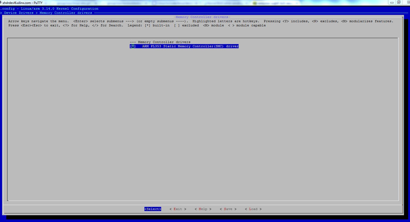
The following kernel configuration options should be enabled for compiling the pl353 smc driverDevice Drivers -> Memory Control Drivers -> ARM PL353 Static Memory Controller(SMC) driver
CONFIG_ARM = y
CONFIG_PL353_SMC = y
NAND Driver
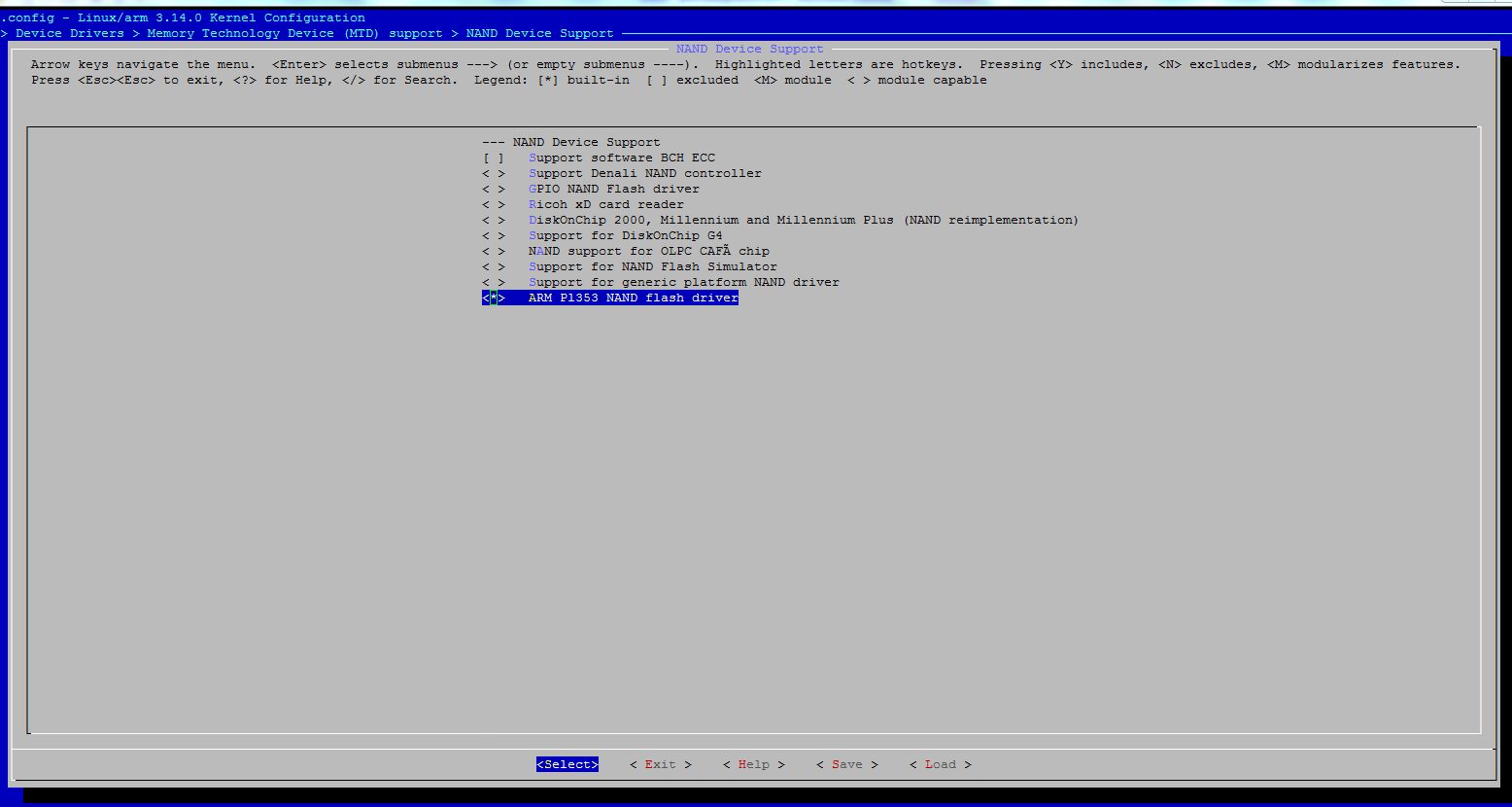
The following kernel configuration options should be enabled for compiling the pl353 smc nand driverDevice Drivers -> Memory Technology Device (MTD) support -> NAND Device Support ->ARM PL353 NAND flash driver
CONFIG_MTD_NAND = y
CONFIG_ARM = y
CONFIG_PL353_SMC = y
CONFIG_MTD_NAND_PL35X = y
NOR Driver
Select the Device Drivers option and then, select Memory Technology Devices (MTD).Finally, choose the RAM/ROM/Flash chip drivers option.
Detect flash chips by common flash interface (CFI) by selecting one of the following:
- For the static build, choose the option <*> Detect flash chips by Common Flash Interface (CFI).
- For build as a module, choose the option <M> Detect flash chips by Common Flash Interface (CFI).
- For static build, choose the option <*> Support for AMD/Fujitsu flash chips.
- For build as a module, choose the option <M> Support for AMD/Fujitsu flash chips.
- For static build, choose the option <*> Support for Intel/Sharp flash chips.
- For build as a module, choose the option <M> Support for Intel/Sharp flash chips.
- For static build, <*> Flash device in physical memory map based on OF description
- For build as a module, <M> Flash device in physical memory map based on OF description


Device Tree
For more details on nand devicetree details, please refer Documentation/devicetree/bindings/mtd/nand.txtLink: Device Tree Binding info
The timing parameters t0, t1, t2, t3, t4, t5, t6 denotes
nand-cycle-t0 : Read cycle time(t_rc).
nand-cycle-t1 : Write cycle time(t_wc).
nand-cycle-t2 : re_n assertion delay(t_rea).
nand-cycle-t3 : we_n de-assertion delay(t_wp).
nand-cycle-t4 : Status read time(t_clr)
nand-cycle-t5 : ID read time(t_ar)
nand-cycle-t6 : busy to re_n(t_rr)
NAND Node:
--------------
		smcc: memory-controller@e000e000 {
			#address-cells = <1>;
			#size-cells = <1>;
			status = "disabled";
			clock-names = "memclk", "apb_pclk";
			clocks = <&clkc 11>, <&clkc 44>;
			compatible = "arm,pl353-smc-r2p1", "arm,primecell";
			interrupt-parent = <&intc>;
			interrupts = <0 18 4>;
			ranges ;
			reg = <0xe000e000 0x1000>;
			nand0: flash@e1000000 {
				status = "disabled";
				compatible = "arm,pl353-nand-r2p1";
				reg = <0xe1000000 0x1000000>;
				#address-cells = <1>;
				#size-cells = <1>;
				/* Depending upon the ecc support, change nand-ecc-mode to "hw" */
 				nand-ecc-mode = "on-die";
				/* Depending upon the bus width configuration change it to 8 or 16 */
				nand-bus-width = <8>;
                partition@nand-fsbl-uboot {
                    label = "nand-fsbl-uboot";
                    reg = <0x0 0x100000>;
                };
                partition@nand-linux {
                    label = "nand-linux";
                    reg = <0x100000 0x500000>;
                };
                partition@nand-device-tree {
                    label = "nand-device-tree";
                    reg = <0x600000 0x20000>;
                };
                partition@nand-rootfs {
                    label = "nand-rootfs";
                    reg = <0x620000 0x5E0000>;
                };
                partition@nand-bitstream {
                    label = "nand-bitstream";
                    reg = <0xC00000 0x400000>;

                };

            } ;
        } ;

NOR node:
---------
		smcc: memory-controller@e000e000 {
			#address-cells = <1>;
			#size-cells = <1>;
			status = "disabled";
			clock-names = "memclk", "apb_pclk";
			clocks = <&clkc 11>, <&clkc 44>;
			compatible = "arm,pl353-smc-r2p1", "arm,primecell";
			interrupt-parent = <&intc>;
			interrupts = <0 18 4>;
			ranges ;
			reg = <0xe000e000 0x1000>;
			nor0: flash@e2000000 {
				status = "disabled";
				compatible = "cfi-flash";
				reg = <0xe2000000 0x2000000>;
	           	bank-width = <1>;
           		xlnx,sram-cycle-t0 = <0xb>;
           		xlnx,sram-cycle-t1 = <0xb>;
           		xlnx,sram-cycle-t2 = <0x4>;
           		xlnx,sram-cycle-t3 = <0x4>;
           		xlnx,sram-cycle-t4 = <0x3>;
          		xlnx,sram-cycle-t5 = <0x3>;
           		xlnx,sram-cycle-t6 = <0x2>;
           		#address-cells = <1>;
           		#size-cells = <1>;
           		partition@nor-fsbl-uboot {
                  label = "nor-fsbl-uboot";
                  reg = <0x0 0x100000>;
           		};
           		partition@nor-linux {
                   label = "nor-linux";
                   reg = <0x100000 0x500000>;
           		};
           		partition@nor-device-tree {
                   label = "nor-device-tree";
                   reg = <0x600000 0x20000>;
           		};
            		partition@nor-rootfs {
                   label = "nor-rootfs";
                   reg = <0x620000 0x5E0000>;
            		};
           		partition@nor-bitstream {
                   label = "nor-bitstream";
                   reg = <0xC00000 0x400000>;
            	} ;
			};
        } ;
Performance
| Mode | Write Speed | Read Speed |
| 8 bit | 8MB/sec | 9.5MB/sec |
| 16bit | 7MB/sec | 11.1MB/sec |
Test Procedure
JFFS2 filesystem
How to Run
Erase the flash partition:

flash_eraseall <device>

Mount the partition:

mount -t jffs2 <block device> <directory>

Perform file read/write and compare operation:

unmount the partition:
umount <directory>
UBIFS file system
Images:
Flashcp
flashcp -v <device name>
mtd_speedtest
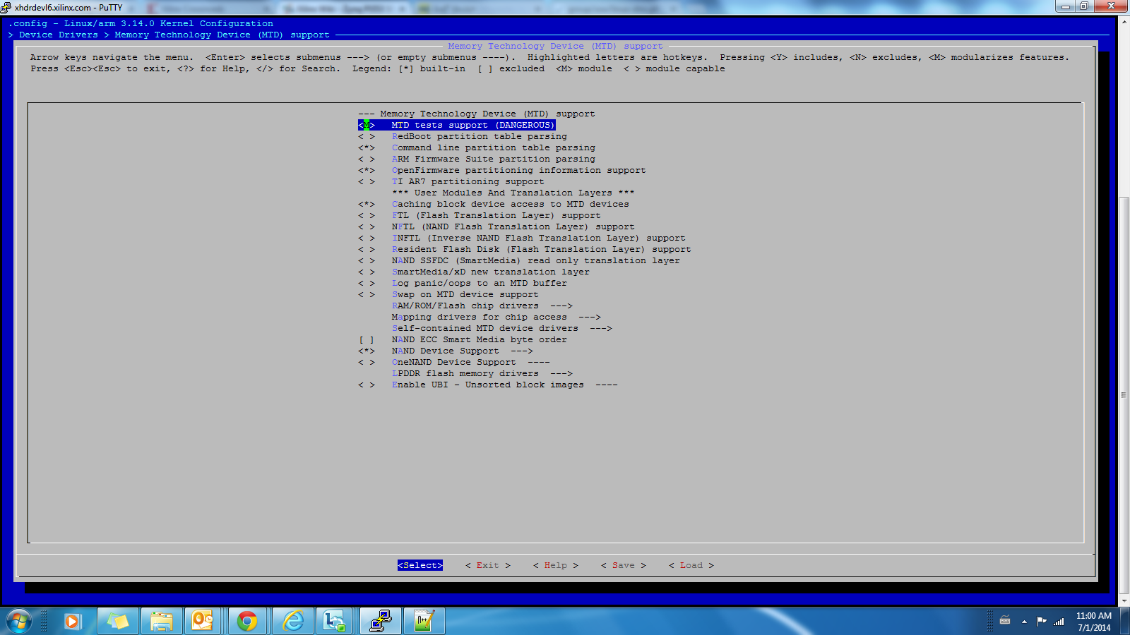
Select the mtd_speedtest from the kernel configuration menu:
Build it as module and use the generated .ko from the location drivers/mtd/tests/
How to run
Speed Test
insmod mtd_speedtest.ko -device=<mtd device number>

rmmod mtd_speedtest
Expected Output
root@xilinx-zc702-2020_1:~# insmod /lib/modules/`uname -r`/kernel/drivers/mtd/tests/mtd_speedtest.ko dev=1

=================================================
mtd_speedtest: MTD device: 1
mtd_speedtest: MTD device size 5242880, eraseblock size 131072, page size 2048, count of eraseblocks 40, pages per eraseblock 64, OOB size 64
mtd_test: scanning for bad eraseblocks
mtd_test: scanned 40 eraseblocks, 0 are bad
mtd_speedtest: testing eraseblock write speed
mtd_speedtest: eraseblock write speed is 8025 KiB/s
mtd_speedtest: testing eraseblock read speed
mtd_speedtest: eraseblock read speed is 9534 KiB/s
mtd_speedtest: testing page write speed
mtd_speedtest: page write speed is 7925 KiB/s
mtd_speedtest: testing page read speed
mtd_speedtest: page read speed is 9499 KiB/s
mtd_speedtest: testing 2 page write speed
mtd_speedtest: 2 page write speed is 7962 KiB/s
mtd_speedtest: testing 2 page read speed
mtd_speedtest: 2 page read speed is 9516 KiB/s
mtd_speedtest: Testing erase speed
mtd_speedtest: erase speed is 170666 KiB/s
mtd_speedtest: Testing 2x multi-block erase speed
mtd_speedtest: 2x multi-block erase speed is 341333 KiB/s
mtd_speedtest: Testing 4x multi-block erase speed
mtd_speedtest: 4x multi-block erase speed is 341333 KiB/s
mtd_speedtest: Testing 8x multi-block erase speed
mtd_speedtest: 8x multi-block erase speed is 341333 KiB/s
mtd_speedtest: Testing 16x multi-block erase speed
mtd_speedtest: 16x multi-block erase speed is 341333 KiB/s
mtd_speedtest: Testing 32x multi-block erase speed
mtd_speedtest: 32x multi-block erase speed is 341333 KiB/s
mtd_speedtest: Testing 64x multi-block erase speed
mtd_speedtest: 64x multi-block erase speed is 341333 KiB/s
mtd_speedtest: finished
=================================================
root@xilinx-zc702-2020_1:~#
oob test
insmod mtd_oob.ko -device=<mtd device number>

rmmod mtd_speedtest
Expected Output
root@xilinx-zc702-2020_1:~# insmod /lib/modules/`uname -r`/kernel/drivers/mtd/tests/mtd_oobtest.ko dev=1

=================================================
mtd_oobtest: MTD device: 1
mtd_oobtest: MTD device size 5242880, eraseblock size 131072, page size 2048, count of eraseblocks 40, pages per eraseblock 64, OOB size 64
mtd_test: scanning for bad eraseblocks
mtd_test: scanned 40 eraseblocks, 0 are bad
mtd_oobtest: test 1 of 5
mtd_oobtest: writing OOBs of whole device
mtd_oobtest: written up to eraseblock 0
mtd_oobtest: written 40 eraseblocks
mtd_oobtest: verifying all eraseblocks
mtd_oobtest: verified up to eraseblock 0
mtd_oobtest: verified 40 eraseblocks
mtd_oobtest: test 2 of 5
mtd_oobtest: writing OOBs of whole device
mtd_oobtest: written up to eraseblock 0
mtd_oobtest: written 40 eraseblocks
mtd_oobtest: verifying all eraseblocks
mtd_oobtest: verified up to eraseblock 0
mtd_oobtest: verified 40 eraseblocks
mtd_oobtest: test 3 of 5
mtd_oobtest: writing OOBs of whole device
mtd_oobtest: written up to eraseblock 0
mtd_oobtest: written 40 eraseblocks
mtd_oobtest: verifying all eraseblocks
mtd_oobtest: verified up to eraseblock 0
mtd_oobtest: verified 40 eraseblocks
mtd_oobtest: test 4 of 5
mtd_oobtest: attempting to start write past end of OOB
mtd_oobtest: an error is expected...
mtd_oobtest: error occurred as expected
mtd_oobtest: attempting to start read past end of OOB
mtd_oobtest: an error is expected...
mtd_oobtest: error occurred as expected
mtd_oobtest: attempting to write past end of device
mtd_oobtest: an error is expected...
mtd_oobtest: error occurred as expected
mtd_oobtest: attempting to read past end of device
mtd_oobtest: an error is expected...
mtd_oobtest: error occurred as expected
mtd_oobtest: attempting to write past end of device
mtd_oobtest: an error is expected...
mtd_oobtest: error occurred as expected
mtd_oobtest: attempting to read past end of device
mtd_oobtest: an error is expected...
mtd_oobtest: error occurred as expected
mtd_oobtest: test 5 of 5
mtd_oobtest: writing OOBs of whole device
mtd_oobtest: written up to eraseblock 0
mtd_oobtest: written up to eraseblock 0
mtd_oobtest: written 39 eraseblocks
mtd_oobtest: verifying all eraseblocks
mtd_oobtest: verified up to eraseblock 0
mtd_oobtest: verified 39 eraseblocks
mtd_oobtest: finished with 0 errors
=================================================
root@xilinx-zc702-2020_1:~#
Change Log
2016.3
- Summary
- None
- Commits
- None
- Summary
2016.4
- Summary
- None
- Commits
- None
- Summary
2017.1
- Summary
- Update smc nand driver as per latest kernel changes
- Commits
- Summary
2017.2
- Summary
- None
- Commits
- None
- Summary
2017.3
- Summary
- None
- Commits
- None
- Summary
2017.4
- None
2018.1
- Summary
- Do bit operations on offset not on virtual address
- Commits
- Summary
2018.2
- Summary
- Fix for incorrect ooblayout offset update
- Commits
- Summary
2018.3
2019.1
- Summary
- Implemented →exec_op
- Commits
- Summary
2019.2
- Summary
- None
- Commits
- None
- Summary
2020.1
- Summary
- Updated the driver as per new kernel NAND framework
- Commits
- 75721e47 updated the driver under new NAND framework
- Summary
Mainline Status
PL353 SMC Driver - DonePL353 NAND Driver - Not Done
http://infocenter.arm.com/help/topic/com.arm.doc.ddi0380g/DDI0380G_smc_pl350_series_r2p1_trm.pdf
References
Pl350 TRM:http://infocenter.arm.com/help/topic/com.arm.doc.ddi0380g/DDI0380G_smc_pl350_series_r2p1_trm.pdf