Zynq-7000 AP SoC SATA part 5 – Building the Design Example
Zynq SATA Storage Extension (Zynq SSE) Developers Guide
Table of Contents
- Describes the items delivered as part of the Zynq SSE.
- Gives an architectural overview over the Zynq SSE.
- Shows the Xilinx Vivado FPGA design flow for Zynq SSE.
- Explains how to activate the MLE license keys for Zynq SSE.
The Zynq SSE is delivered as a complete reference design for the Xilinx Zynq-7000 SoC (Zynq), and effectively extends Zynq with one single SATA host port for HDD and/or SSD storage connectivity.
To ease integration work, Zynq SSE provides a complete FPGA design project for Xilinx Vivado targeting the Avnet Zynq Mini-ITX-7045 Board (Avnet Mini-ITX).
This enables you to quickly bring up Zynq SSE on a known-good FPGA and hardware platform, and to migrate Zynq SSE to your particular target system. Please refer to the following MLE Technical Briefs for further information:
- TB20140428 Zynq SSE basic setup for Avnet Mini-ITX.
- TB20140429 Zynq SSE benchmarking for the Avnet Mini-ITX.
http://MLEcorp.com/ZynqSSE
1 Delivered Items
Zynq SSE is delivered inside an installable archive for Windows, 32 bit Linux, and 64 bit Linux. Inside this archive you will find the following files.To obtain this file, go to http://mlecorp.com/zynqsse and fill out the Contact Request Form.
| Files Provided | |
| zynqsse.zip | Complete Vivado 2014.3 design project targeting the Avnet Mini-ITX. |
| BOOT.bin | Compilation of Bitstream, FSBL and U-Boot, all targeted for Avnet Mini-ITX. |
| Image.ub | Linux Ramdisk Image with MLE SATA extensions including the Zynq SSE Linux kernel modules. |
| sata_driver.zip | Archive with Zynq SSE Linux kernel modules, as running in PetaLinux system, and as they need to be installed in your target system. |
| U-Boot.elf | U-Boot Bootloader to get Petalinux running. |
| fsbl.elf | First Stage Boot Loader, with SATA ICAP patch (refer to Section 3.4). |
http://MLEcorp.com/US-license
For additional information about the Avnet Mini-ITX board, please refer to the MLE Technical Brief TB20140428, or visit Avnet’s product webpage at:
Avnet Mini ITX
2 Setup of Hardware Platforms for Zynq SSE
Ready-to-run Evaluation Reference Designs (ERD) for Zynq SSE are available the Avnet Zynq Mini-ITX-7Z045 Board (Avnet Mini-ITX), shown in Figure 3. For easy diagnostics Zynq SSE uses on-board LEDs.2.1 LED Description
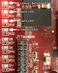
Status LEDs can be found next to the PCIe connector. The associated meanings can be seen in the following table:| D7 | Timeout LED, indicates that the run-time license expired. |
| D6 | Gen3 Link, indicates 6 GBit/s connection. |
| D5 | Gen2 Link, indicates 3 GBit/s connection. |
| D4 | Linkup and Activity, LED will light up on Linkup and will go dark during data transfers. |
Figure 1: Location of the User LEDs on the Avnet Mini ITX Board
Figure 3: Zynq SSE Hardware Setup for Avnet Mini-ITX
3 Architecture Details
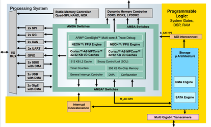
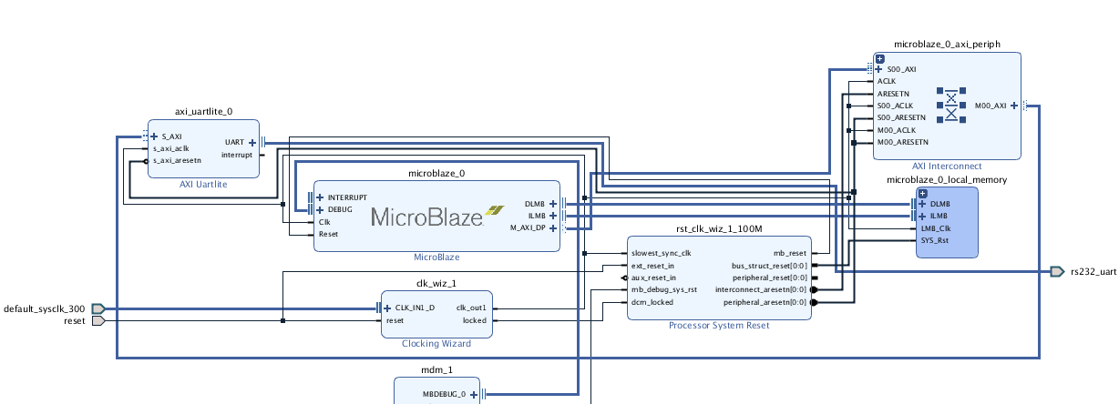
The system architecture diagram in Figure 5 gives an overview of the Zynq SSE reference design: Within the Zynq Programmable Logic (PL) the MLE Storage Micro-Architecture instantiates the DMA and the SATA Host Controller IP blocks. The storage micro-architecture itself interfaces with the Zynq Processing System (PS) via the AXI Interconnect. The ARM A9 in the PS runs Xilinx PetaLinux and the SATA Linux kernel drivers. Please note that this figure is not to scale and that there is plenty of programmable logic resources left for you in the Zynq FPGA device to implement your portions of your target design! The block diagram in Figure (for the Avnet Mini-ITX) provides more details of the Storage Micro-Architecture. To ease integration of Zynq SSE into your target system, the Storage Micro-Architecture assembles all 3rd-party IP cores, instantiates and parameterizes them in accordance to the original IP core vendor’s design manual, wires them up properly, and implements all connectivity to internal signals as well as to external FPGA IO. All of this is encapsulated into one top-level module mle_storage_uarch. Further down, we provide details on how system software parameters and memory addresses have been set.Figure 5: Zynq SSE System Architecture
3.1 Pin Assignments for the Avnet Mini-ITX
As external IO, the Storage Micro-Architecture connects to the following FPGA pins to establish SATA connectivity and to provide user LEDs for diagnostic purposes. For your convenience Figure 1 identifies LEDs on the Avnet Mini-ITX-7045 board (for Mini-ITX-7045 hardware revision 1.1, and newer).Figure 6: MLE Storage Micro-Architecture Details for Avnet Mini-ITX
| Name | Direction | Description |
| sata_ref_clk_p_i sata_ref_clk_n_i | in in | Incoming Reference Clock |
| sata_rxn_i sata_rxp_i | in in | SATA Rx Pair differential |
| sata_txn_o sata_txp_o | out out | SATA Tx Pair differential |
| sata_clkin_p_o sata_clkin_n_o | out out | SATA Clock differential |
| sata_led_linkup_o | out | Illuminates when SATA link is established; goes dark when data is read or written from the SATA disk |
| sata_led_gen2_o | out | Illuminates when SATA 3 Gbps speed is established. |
| sata_led_gen3_o | out | Illuminates when SATA 6 Gbps speed is established. |
| sata_led_timeout_o | out | Illuminates when Zynq SSE license has expired. |
ATTENTION!
Please keep in mind that this design project targets the Avnet Mini-ITX-7Z045 and that you need to change those pin assignments to match your target hardware setup!
3.2 AXI Memory Interfaces
According to Figure 6, the Storage Micro-Architecture connects to the Zynq PS via four AXI interconnects. The interfaces for the Storage Micro-Architecture have been pre-configured with the following memory address space:| Name | Offset Address | High Address | Description |
| M_AXI | 0x00000000 | 0x3FFFFFFF | AXI master for direct memory access into the DDR3 RAM attached to the Zynq PS |
| S_AXI_L_SATA | 0x41000000 | 0x4100FFFF | AXI-lite interface to control the SATA host controller IP core |
| S_AXI_L_DMA | 0x41010000 | 0x4101FFFF | AXI-lite interface to control the DMA controller IP core |
| S_AXI_L_TB | 0x41020000 | 0x4102FFFF | AXI-lite interface to control the micro-architecture and for production license key activation |
ATTENTION!
The entire memory address space between 0x41000000 and 0x4102FFFF is fixed and reserved for Zynq SSE. You must ensure that you do not conflict with this memory address space, and, in particular, that you do not write into that memory address space. You must not change those address values or Zynq SSE stops functioning as specified!
3.3 IEEE 1275 Device Tree
The memory address setting are also reflected in the device tree. This device tree is stored inside the image.ub file. The following snippet shows the Zynq SSE specific section:satah_0_hc: satahc@41000000
{compatible = "aws,satah4-1.00.a";
reg = <0x41000000 0x800>;
interrupt-parent = <&&ps7_scugic_0>;
interrupts = <0 58 1>;
dma-engine = <&&satah_0_dma 0>; };
satah_0_dma: dmaeng@41010000
{compatible = "aws,axi-dma-1.00.a";
reg = <0x41010000 0x800>;
interrupt-parent = <&&ps7_scugic_0>;
interrupts = <0 59 4>; };
mle_ipwatch: ipwatch@41020000
{compatible = "mle,axi-ip-watch-1.00";
reg = <0x41020000 0x1000>; };
3.4 Bootloader Settings
To ensure that Zynq SSE runs on a supported device, Zynq SSE will check for your FPGA’s device ID. To do this the ICAP interface is used. However, the ICAP interface will only work if the PCAP interface has been deactivated. This has been done by MLE by running a modified First Stage Bootloader (FSBL), which is a transparent change because the PCAP interface will be activated again by the U-Boot, later.We recommend that you to use the FSBL from MLE. If you need to use your own customized FSBL (maybe, because you need to initialize your own hardware blocks) please make sure to adjust your FSBL by editing the function FsblHookBeforeHandoff in the file SDK_Export/fsbl/src/fsbl_hooks.c as shown below.
u32 FsblHookBeforeHandoff(void)
{
  u32 Status;

  u32 xdcfg_ctrl;
  int status;
  XDcfg xdcfg_instance;
  XDcfg_Config *ConfigPtr;

  Status = XST_SUCCESS;
  ConfigPtr = XDcfg_LookupConfig(XPAR_PS7_DEV_CFG_0_DEVICE_ID);
  status = XDcfg_CfgInitialize(&&xdcfg_instance, ConfigPtr, ConfigPtr->BaseAddr);
  if (status != XST_SUCCESS) {
    return XST_FAILURE;
  }
  xdcfg_ctrl = XDcfg_ReadReg(xdcfg_instance.Config.BaseAddr, XDCFG_CTRL_OFFSET);
  xdcfg_ctrl &&= ~XDCFG_CTRL_PCAP_PR_MASK;
  XDcfg_WriteReg(xdcfg_instance.Config.BaseAddr, XDCFG_CTRL_OFFSET, xdcfg_ctrl);

  /*
   * User logic to be added here.
   * Errors to be stored in the status variable and returned
   */
  fsbl_printf(DEBUG_INFO,"In FsblHookBeforeHandoff function \r\n");

  return (Status);
}
ATTENTION!
Please make sure that this code is executing on startup of the system. If not, Zynq SSE will not work!
4 Zynq SSE Design Flow
Typically, integrating a 3rd-party IP core requires reading a lot of documentation to properly parameterize and instantiate the IP core into your target design. To reduce your design effort when integrating Zynq SSE, MLE provides you with a complete reference design project. This reference design runs on the Avnet Mini-ITX-7Z045 which makes system-level verification and software development easy. To port this reference design to your target system, please follow the three simple rules of “Things You Must Do, Things You Can Do, and Things You Must Not Do”.4.1 Things You Must Do
Xilinx Vivado offers an innovative new design flow via the so-called “Run”. To migrate the Zynq SSE Reference Design to your target system, please create a new “Run”, where you will have to specify your particular part from the Zynq-7000 family, including picking the proper speed-grade, device and constraints.You must also adjust the pin assignments in the Design Constraints.
You must further supply a SATA-capable differential reference clock with low jitter at 150 MHz to the following pins:
sata_ref_clk_n_i sata_ref_clk_p_i
On the software side you must install the MLE Linux kernel modules into your target system. You can copy them from your Avnet Mini-ITX-7Z045 system, or extract them from the separate archive mlelkm.tar which we provided for your convenience.
To compile Zynq SSE under Xilinx Vivado you must have a compile-time license key. This is described in Section 5.1.
4.2 Things You Can Do
You can add pretty much any additional functionality to the PS and/or PL. Zynq SSE does not require exclusive access to the AXI ports, so you can share those with the AXI Interconnect for your user logic. Obviously, you should follow good design practice when sharing resources to not create bottlenecks which may impact your SATA performance.You can also leave out the four user LEDs (sata_led) as they are provided solely for convenient diagnostic purposes. It is okay to leave those LED outputs open in your target design.
4.3 Things You Must Not Do
Most importantly, you must not change the setup of the memory address space of the MLE Storage Micro-Architecture. This is so important, that we repeat this here, again!And, you must not pick any target FPGA device other than those devices with multi-gigabit transceivers from the Xilinx Zynq-7000 SoC family as Zynq SSE will not run without it. This has legal and technical reasons because MLE’s Storage Micro-Architecture for Zynq SSE is designed and licensed for Zynq only.
4.4 Running Zynq SSE in Xilinx Vivado
Zynq SSE has been tested (under Windows and Linux) for:Xilinx 2014.3 Vivado
Xilinx 2014.3 SDK
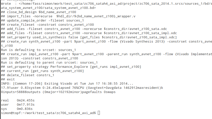
First of all extract the archive zynq_sse.zip. This folder does not yet contain any Vivado project sources. They have to be created first using the build script build.sh inside the top folder zynq_sse_avnet_7045. This build script has to be executed inside a Xilinx shell. Please make sure you have the proper Xilinx Vivado version installed. And make sure that you set the executable flag for the build script by executing chmod +x. If this was successful you will receive an output similar to the following:
Figure 8: Build of the Vivado Project
After executing the build script, the Vivado project and the block design will have been generated. You will find a new folder project in your zynq_sse_avnet folder. Open this folder and verify that it contains the folders and Vivado project files displayed below.
project/zynq_sse_sata_2014.3.cache/
project/zynq_sse_sata_2014.3.srcs/
project/zynq_sse_sata_2014.3.xpr
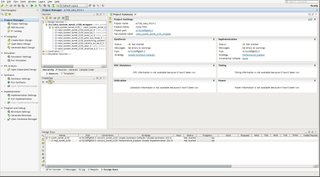
Click on Open Block Design and you will see the Block Design, shown in Figure 10:
Figure 9: Vivado Startup Screen
Figure 10: Block Design
This is where you can add your own design blocks to Zynq SSE. You can add additional AXI-ports and AXI-interconnects for your additional hardware blocks. By clicking on the Address Editor you will see the offsets of the different AXI-Interfaces. Please make sure that they match the values from Section 3.3.
At this point you will be able to generate your own bitfile. This is required to build your BOOT.BIN. To do this click on the Generate Bitstream Button or via the menu: Flow -> Generate Bitstream
Once this successfully completes, you will have a bitfile in the folder: zynq_sse_sata_2014.3.runs/impl_avnet. Using this bitfile you can generate the file BOOT.BIN.
To do this open a Petalinux version 2013.04 shell. You will need the U-Boot.elf and the fsbl.elf file. We recommend that you to use the pre-built files and delivered by MLE (in the pre-compiled folder), however, it is also okay to use your own customized files. Just make sure you have made the necessary adjustments described in Section 3.4.
Once you have all the files needed you can create your BOOT.BIN file with the following command:
petalinux−gen-zynq−boot −b <path to fsbl.elf> −f <path to bitfile> −u <path to u−boot.elf> −o ./BOOT −−force
Now copy your BOOT.BIN and your image.ub file onto a FAT32 formatted SD-Card. After you have followed the instructions for setting up your target hardware, you will have a fully functional Zynq SSE!
Document History
| Date | Author | Revision |
| 2014-03-25 | CG | Initial draft document |
| 2014-05-19 | SL | Added licensing concepts |
| 2014-06-17 | SL | Updated Vivado design flow |
| 2014-06-30 | ES | Update for ZynqSSE Release 1.2 |
| 2014-12-5 | AS | Update for Vivado 2014.3 |
© Copyright 2019 - 2022 Xilinx Inc. Privacy Policy
