Zynq UltraScale+ MPSoC - System Performance Modelling
Table of Contents
Document History
| Date | Version | Author | Description of Revisions |
| 12/6/2017 | 0.1v | E.Srikanth | Initial Version |
Summary
This application note educates users on the evaluation, measurement, and modeling of the performance of the Zynq UltraScale+ MPSoC. The application note introduces and explains an example design that shows the different aspects of the system performance of Zynq UltraScale+ MPSoC devices. The design highlights the communication between the programmable logic (PL) and the processing system (PS) in the Zynq UltraScale+ MPSoC architecture. The design also allows you to model the system to evaluate if the Zynq MPSoC meets your system performance needs. The design that is provided with this application note is the same System Performance Modeling (SPM) project that is provided in SDK and documented in SDK User Guide: System Performance Analysis (UG1145) [Ref 1] for Zynq UltraScale+ MPSoC.
An SPM project is executed in actual target hardware and includes a fixed bitstream containing eight AXI traffic generators. These traffic generators are configurable cores used by SDK to model programmable logic (PL) traffic activity. Software applications can also be run simultaneously in the processing system (PS), and you can specify system configuration parameters. After a user has run an SPM project and would like to extend it to better reflect their application, the design in this Technical Article can be used.
Implementation
| Implementation Details | |
| Design Type | PS & PL |
| SW Type | Standalone |
| CPUs | Quad Core Cortex-A53 |
| PS Features | PS-PL Interfaces, ACP, OCM, DDR |
| PL Cores | AXI Traffic Generators, AXI Performance Monitors |
| Boards/Tools |
|
| Xilinx Tools Version | Vivado 2017.1, Vivado 2017.2 |
| Other Details | |
| Address Maps | |||
| Base_Address | Size | Interface | |
| atg_hpc0 | 0xA0000000 | 1M | S_AXI |
| atg_hpc1 | 0xA0100000 | 1M | S_AXI |
| atg_hp0 | 0xA0200000 | 1M | S_AXI |
| atg_hp1 | 0xA0300000 | 1M | S_AXI |
| atg_hp2 | 0xA0400000 | 1M | S_AXI |
| atg_hp3 | 0xA0500000 | 1M | S_AXI |
| atg_acp | 0xA0600000 | 1M | S_AXI |
| atg_lpd | 0xA0800000 | 1M | S_AXI |
| axi_pmon | 0xA0900000 | 1M | S_AXI |
| S No | Downloads | |
| 1. | System Performance Modeling design for 2017.1 | zcu102_spm_design_2017_1.zip |
| 2 | System Performance Modeling design for 2017.2 | zcu102_spm_design_2017_2.zip |
Introduction
There are three major sections of this application notes.
- The first section describes the system performance of a Zynq UltraScale+ MPSoC.
- The second section shows you how to:
- Implement a system model of a design using a PL implementation that emulates an application.
- Use the Software Development Kit (SDK) to show system performance metrics using the model.
- The third section shows you how to
- Add your own software to run the model.
- Replace items in the PL with your own IP
Zynq UltraScale+ MPSoC Performance
The performance of a SoC is measured at the device or system level, not at the interface or circuit block level. A primary component that determines performance is how effectively the system architecture handles shared resource contention. The connected blocks typically include the application processor unit (APU), interconnect, I/O peripherals, I/O, and memory controllers (static and dynamic) (Figure 1).
Another important factor is the speed at which these blocks operate and the traffic they generate. These blocks can be grouped into subsystems such as the application processor unit, I/O subsystem, and memory subsystem.
The memory subsystem, especially on Zynq UltraScale+ MPSoC, is the most critical shared resource subsystem that determines the SoC performance.
Some of the factors affecting system performance are:
- Cache sizes
- Memory speed
- Memory efficiency
- Memory data width
- CPU speed
- Interconnect
- Integration of the blocks
Some of these factors are constant and cannot be changed. Others are part dependent, some are platform dependent, and others are design dependent. It is important to define how efficiency and effectiveness are used in this document:
Efficiency refers to how efficiently the memory controller uses the DRAM. An efficient memory controller uses DRAM intelligently to get more bandwidth. The bandwidth is measured in MB/s and efficiency is measured as a percentage.
Effectiveness refers to how effectively the DRAM controller distributes the memory bandwidth. Or, another way to look at this is the “fairness” of the DDR controller giving bandwidth to the different ports. In other words, the efficiency is how much bandwidth the controller gets from the theoretical maximum, and the effectiveness is how that bandwidth is distributed to the contending blocks.
Figure 2 shows the most important factors to consider for system performance. One of the important things an SoC needs to do is to keep the CPU running with a minimal number of data-dependent stalls. To achieve this, data used by the CPU need to be loaded to the caches, which has much lower access latency than the main memory. The speed at which data can be loaded into the cache depends on the performance of the memory subsystem. For example, if the bandwidth of the memory subsystem is deficient, caches are not filled on time and the CPU stalls waiting for the data.
The performance of a memory subsystem mainly depends on:
- Speed (frequency) of the memory
- Efficiency of the DRAM controller
- Effectiveness of the DRAM controller
- Width of the memory interface (both internal and external)
- Ports to the DDR controller (internal)
- Interfaces to the DRAM (through the PHY – external)
Note: The memory subsystem does not include the caches.
If the memory subsystem in an SoC does not have enough bandwidth, the performance of the whole system is negatively affected. For example, if the CPU is operating at a high frequency and is trying to fetch more data from the memory than the level-2 cache is able to deliver in a timely manner, the CPU has to stall until the data is received. In this kind of system, having a CPU with a higher clock speed alone does not increase the performance of the system because the memory subsystem is the bottleneck.
Figure 3 shows the other factors in system performance. Typically, an SoC is a heterogeneous system and contains blocks that generate different types of traffic. All these blocks compete for the same memory resources. The memory subsystem must be intelligent enough to resolve contention of resources between different circuit blocks and handle different types of traffic efficiently and fairly. Therefore, comparing CPU clock rates without taking into account other elements in the SoC (specifically the memory subsystem and the programmable logic) is of limited value and could potentially paint a very misleading picture.
Some of the different types of traffic in Zynq-7000 AP SoCs are between the following masters and the DDR:
- Traffic from the APU (memory load and store instructions from the CPU and direct memory access (DMA) requests from the central DMA)
- PS peripherals (Ethernet, USB, etc.)
- DMA requests originated from the PL
- PL peripherals (IP and accelerators).
For example, the video pipeline IP. The memory subsystem must arbitrate access requests from these different traffic sources while maximizing bandwidth utilization of the DRAM. An effective memory controller exhibits balanced and predictable behaviors. Fairness of the memory controller is modulated by the quality of service (QoS) mechanism, which optimizes total throughput while avoiding starvation of any individual traffic. An unfair implementation of a memory subsystem would be based on an absolute arbitration priority. This type of arbitration is inappropriate in an SoC where multiple data streams from different sources need to be supported at the same time and starvation at any source almost always slows down the overall system.
Design Details
An Instrumented Design for Performance Analysis to model a system that uses the Zynq UltraScale+ MPSoC, you need a design that can emulate the data traffic from the PL to the PS. This is done using Xilinx IP that can be configured to mimic different parts of a user design. See Reference Design to download the design files. The design generates traffic from the PL to the PS DDR to emulate an application. To do this, the program uses an IP core called the AXI Traffic Generator (ATG), which is documented fully in the LogiCORE™ IP AXI Traffic Generator v2.0 Product Guide (PG125) [Ref 2]. The ATG can mimic standard interfaces like Ethernet, USB, and PCIe® or be configured in a custom manner to better match a customer application. In this design ATG are configured in Advanced mode that allows full control over the traffic generation. Control registers are provided to program the core and generate different AXI4 transactions. The reference design with this application note contains eight ATGs that are connected to the two high performance cache coherent (HPC)ports, four high-performance (HP) ports, the accelerator coherency port (ACP), and one Low Power Domain port of the Zynq UltraScale+ MPSoC. These ATGs can be configured for different traffic classes and you can change them for the system you would like to model using the SDK tool. This procedure to change the design (specifically the ATGs) to model an application is described in System Performance Analysis
The block diagram of the design (in the Vivado Design Suite) is shown in Figure.
| Figure 1: ZCU102 SPM Block Design |
All eight ATGs are configured with 128bit Master interface which is connected to each of the Slave High performance ports of the Zynq UltraScale+ MPSoC and each ATG runs off an FCLK from the PS and is configured for 250 MHz. The estimated throughput in MB/s for the ATG can be calculated using the below Equation Estimated Throughput= (AXI-Datawidth/8) x PL clock frequency x (Beats per transaction/Max(beats per transaction, Transaction interval)) Another important IP that is added to the design is the AXI Performance Monitor IP that mesures the AXI performance . The LogiCORE™ IP AXI Performance Monitor core enables AXI system performance measurement for multiple slots (AXI4/AXI3/ AXI4-Stream/AXI4-Lite). This core captures configurable real-time performance metrics for throughput and latency for connected AXI interfaces. In addition, the AXI Performance Monitor core logs the AXI transactions, external system events and performs real-time profiling for software applications. There are also four AXI Performance Monitor IPs that are hardened on the Zynq UltraScale+ MPSoC that can monitor the AXI traffic on the Zynq MPSoC Processing system
There are a total of 9 monitor points, monitored by 4 APMs, as follows:
- One 6-slot APM (choose 1 AXI bus to monitor at a time) o AXI buses to DDR controller ports 0 - 5
- One 1-slot APM: o AXI bus from CCI to Core Switch
- One 1-slot APM: o AXI bus from OCM switch to OCM
- One 1-slot APM: o AXI bus from LPD switch to FPD switch, before IDC & AIB
All the APMs in the PS are configured in Advanced mode and the APM in the PL is configured in Profile Mode. The Profile mode shows bandwidth and latency at a high level. SDK reads the APM every 50 ms for the data on each slot or interface. The other modes are for more detailed gathering of data at the interface. The Advanced and Trace modes take data at a higher rate than the Profile mode.
The Base address of the PS APM in the
| Address Map of PS APM | |||
| IP Block | Base Address | Size | Description |
| DDR APM | 0xFD0B0000 | 64K | Monitors AXI buses to DDR controller ports 0 - 5 |
| CCI to Core Switch APM | 0xFD490000 | 64K | MonitorsAXI bus from CCI to Core Switch |
| OCM switch to OCM APM | 0xFFA00000 | 64K | Monitors AXI bus from OCM switch to OCM |
| LPD switch to FPD switch | 0xFFA10000 | 64K | Monitors AXI bus from LPD switch to FPD switch, before IDC & AIB |
The configuration for the PL APM is shown in Figure. Eight interfaces are selected.
Each of the monitor interfaces are set up the same way for AXI4 ports and for 128 bits of data. The first four monitor interface configurations are shown in Figure 7 (these are the two HPC ports and the two HP ports) The second page of the APM configuration page shows connectivity of the other two HP ports and seventh is the ACP, and the eighth is the LPD port.
SDK Performance Tool Box:
The performance analysis toolbox in the Xilinx® Software Development Kit (SDK) offers a set of system-level performance measurements. For a design that targets the Zynq UltraScale+ MPSoC, this includes performance metrics from both the Programmable Logic (PL) and the Processing System (PS).
The PL performance metrics include the following:
• (Write/Read) Transactions – number of AXI transactions
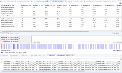
• (Write/Read) Throughput – write or read bandwidth in MB/sec
• Average (Write/Read) Latency – average write or read latency of AXI transactions
The PS performance metrics include the following:
• CPU Utilization (%) – percentage of non-idling CPU clock cycles
• CPU Instructions Per Cycle (IPC) – estimated number of executed instructions per cycle
• L1 Data Cache Access and Miss Rate (%) – number of L1 data cache accesses and the miss rate
• CPU (Write/Read) Stall Cycles Per Instruction - estimated number of stall cycles per instruction due to memory writes (write) and data cache refills (read)
This mix of performance metrics is gathered from different parts of the target and combined into a common timeline and display, enabling system-level performance analysis.
In order to gather and display these metrics, SDK includes a monitor framework that accesses various profile counters across a target system, as well as a host-target communication framework to perform the sampling and offloading of these counters.
The metadata required by SDK to perform this monitoring is exported by Vivado® Design Suite and read by SDK when a Hardware Platform Specification project is created. While this export/import procedure has already been performed for the System Performance Modeling (SPM) project, it can also be executed on your design.
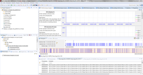
In other words, all of the monitoring and analysis described herein is available and applicable to the SPM design as well as your design. PS Performance Graphs:
Each ARM Cortex-A53 CPU contains a Performance Monitor Unit (PMU). These PMUs are configured to monitor a number of different performance metrics, including CPU utilization and Instructions Per Cycle (IPC). The PMUs are accessed as part of the performance monitor framework used by SDK.
Steps to run the SPM design
- Unzip the zcu102_spm_design_2017_1.zip file on your C drive.
- Start Vivado Design Suite 2017.1 and Open the Tcl window.
Change directories (cd) to the directory where you placed the design files.
Figure: Typing the commands in the TCL console - Source the project tcl file
In the TCL console type the following command.
In case of production silicon source the zcu102_spm_design_2017_1_prod.tcl file
source zcu102_spm_design_2017_1_prod.tcl
In case of ES2 silicon source the zcu102_spm_design_2017_1_es2.tcl file
source zcu102_spm_design_2017_1_es2.tcl
The TCL file will create the SPM project , adds the IP blocks to the IP Integrator and makes the appropriate connections and generate the bit stream file. - After the bit stream generation is complete. The Bitstream generated dialog pops up.
- Select View Reports Option and click OK to close the dialog.
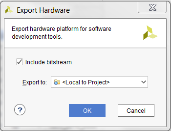
- Select File--> Export Hardware to export the hardware files to SDK.
- .In the Export Hardware Dialog box , check the Include bitstream box and Click on OK.
- Launch SDK command from the Vivado Design Suite.
Select File --> Launch SDK and the SDK Launch is dialog is popped up.
Keep the Options at it defauls and Clock OK to launch SDK.
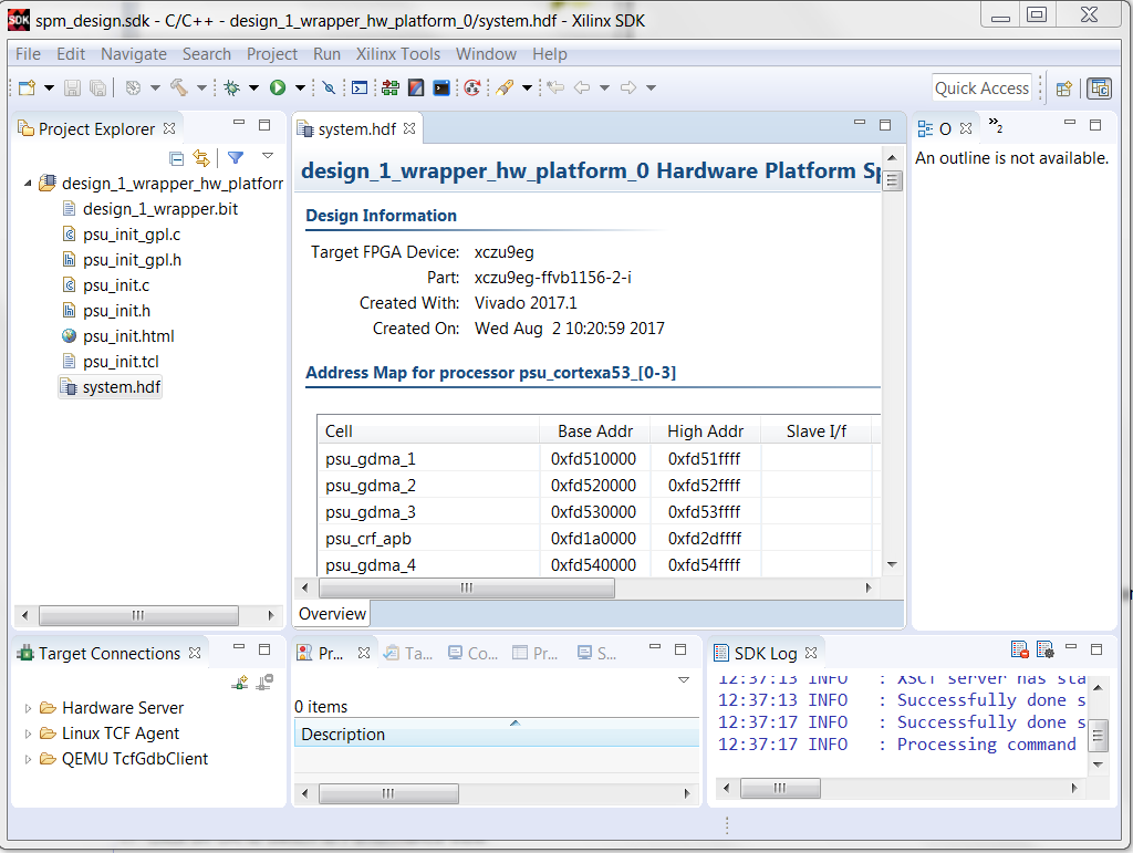
After the SDK tool is launched. The hardware description file along with the bitstream is exported to the SDK. - Close the Welcome Screen to view the exported files in the Project Explorer view of the SDK.
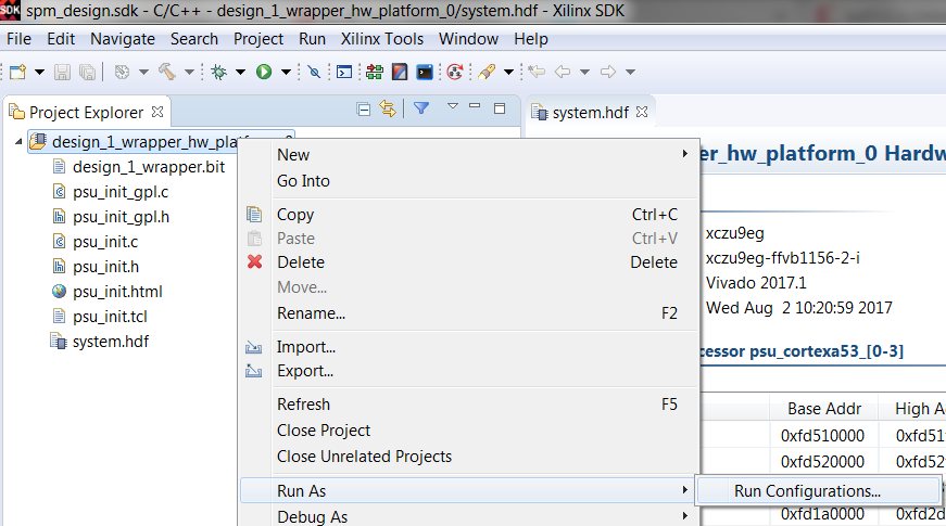
- Right click on the design_wrapper_hw_platform_0 folder in the Project explorer view.
- Click Run As > Run Configurations. This will launch the run configurations dialog.
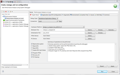
- Double click on Performance analysis to create a new Performance analysis configuration.
- a. Select the Debug Type as Standalone debug.
- b. Check the Reset Entire system Option
- c. Check the Reset APU system
- d. Check the Program FPGA system
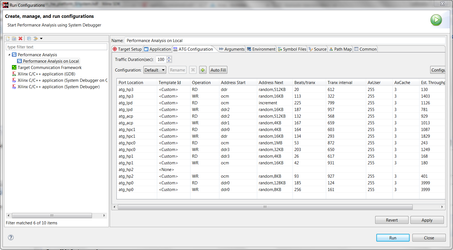
- Click on ATG Configuration and Click on the Auto Fill button.
Note: Please also check the estimated throughput dialog to get an estimate of throughput available per port. - Click on Run to start the Performance Analysis. The SDK will ask switch to Performance Analysis Perspective view.
Click on OK to switch to Performance view. - The SDK window will switch to Performance View as shown below.
- Click On the APM Performance Counters Tab to view the Counter details.
Conclusion:
Using the above steps you will be able to run a custom hardware with ATGs and APMs and monitor performance on Zynq UltraScale+ MPSoC.
© Copyright 2019 - 2022 Xilinx Inc. Privacy Policy
