This page describes the usage of the RFSoC Data Converter Evaluation
Tool Getting Started GuideThe below sections describe the build and run flow tutorial.
| Table of Contents |
|---|
tool, as well as steps to build the hardware and software for the ZCU111 reference design.
Table of Contents
| Table of Contents | ||
|---|---|---|
|
Using the RFSoC Data Converter Tool
UI Flow
Run the RF_DC_Evaluation_UI.exe to launch the UI. The UI Launch page looks as shown in the below figure:
UI Options
In this section, we will go through the major UI menu commands and tabs
Menu
File
File|Load/Save configuration: Configuration here means the settings of the RFSoC block, for example, real or I/Q mode, mixer settings, enable or bypass of internal PLL. All these settings can be saved and restored from a file on a PC.
Configuration files should be placed in \Config\ path with
...
extension .cfg
File| Load/Save preferences: Preferences is the settings of this software UI, including all the tabs that are opened, the mapping in Multi View mode, number of samples.
User can save preferred settings of UI and restore whenever is required.
Preference files should be saved in \Config\ path with
...
extension .prf
File|Export ADC Data: This command exports ADC captured data of selected ADC channels with
...
. lvm
...
file format. The default directory is \Data\ADC\
File|Exit
...
: Exits the software.
Edit
Standard Windows edit menu
Settings
Settings|Communication
...
: Used set your preferred communication protocol and interface.
.jpg?version=1&modificationDate=1545044455635&cacheVersion=1&api=v2&width=400)
...
| Info |
|---|
For this evaluation tool, select Ethernet interface only. |
Settings|Data Folders
Choose your preferred folders for DAC test vector, saved ADC data and on board clocking frequency configuration files. By default, it is under the following path:
\Data\
...
with folder name
...
of ADC,
...
DAC and Clockingrespective.
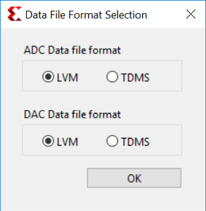
Settings|Data File Format
Choose your preferred file format
...
between lvma and tdms.
...
| Info |
|---|
Sample data files for DAC are located in RFDC_UI_1.0\Data\DAC. |
Window
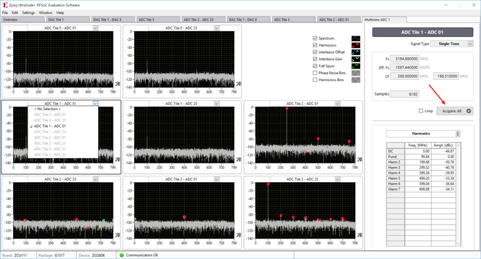
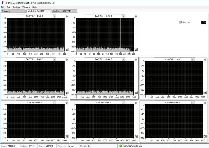
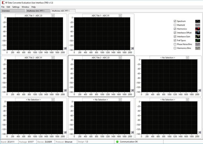
Window | MultiView
MultiView opens all the ADC or DAC FFT plots in their respective pages, with option of selecting channel for each window. Clicking on ’Acquire All’ will update all windows with respective plots.
Window|Commands log
This opens the commands log window. You can dump commands history and API response in this window.
Window|Merge all windows: You can drag any opened tab to a separate window, this command will merge all separate tab to one window.
Help
Help|About: About provide some general information of this Evaluation UI. You can check the version here, which might be needed when building
...
.lvm
...
file.
Tab
Overview
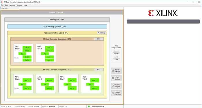
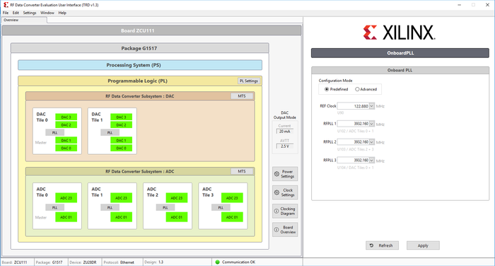
This is the home page of this UI, it shows top level framework of all converters grouped in a tile. User will see this page on UI start up.
On board Clocking, DAC output Voltage, Memory Type and Multi-Tile Sync (MTS)
In Overview tab,
...
click Settings. It will
...
open Onboard PLL and DAC Output Settings UI on the right panel. Evaluation UI provides the option
...
of Predefined and Advanced mode for onboard clock setting.
In predefined mode, available frequencies are provided in a drop-down list for both ADC and DAC. The user can select a sampling frequency and then click on Apply. Evaluation UI will begin programming of onboard RFPLL.
The UI will open by default in BRAM mode. The user has an option to change the memory type between BRAM and DDR modes. Refer to Appendix B Switching between memory types types for the procedure to change memory type.
The UI supports Multi-Tile Synchronization feature which will synchronize all the DAC and ADC channels. Refer
...
to Multi-tile Synchronization (MTS) Run Flow for the procedure to test MTS feature.
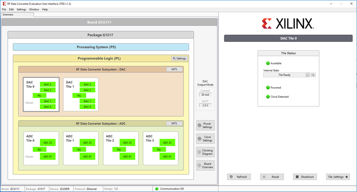
ADC/DAC Tile
...
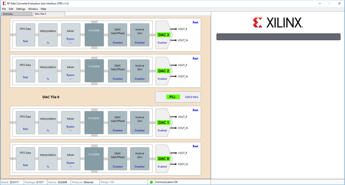
In Overview tab, click any tile of ADC or DAC. This will open the individual tile page as shown below.
In this tab, you can reset, shutdown, start a tile. You can also get current tile status by clicking on the Refresh button.
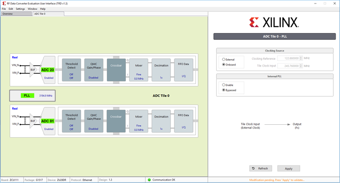
Tile PLL settings
In tile setting page, click on the PLL box, this will open the PLL settings in right panel as shown in below figure. User can choose the clock source of converter tile either from onboard PLL (LMX2594) or output of internal PLL.
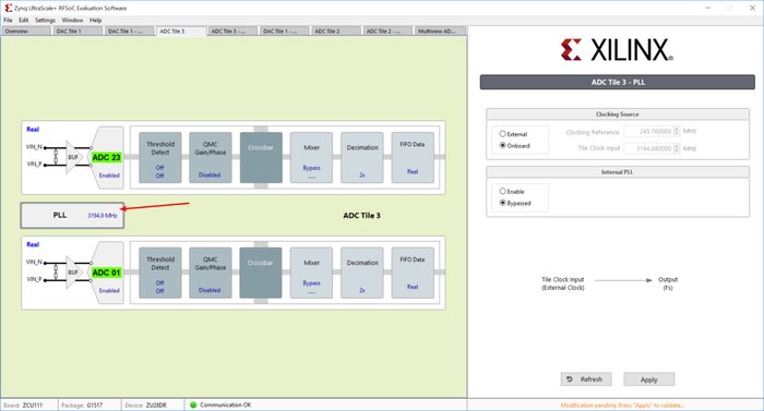
For choosing external clock you need to solder a capacitor on board (refer to UG1271 for more details), feed clock through XM500 daughter card and disable related output from onboard RFPLL. Please make sure correct clock frequency is supplied from external source.
...
| Info |
|---|
0dBm clock power is required to drive RFSoC clock input for specified performance. Insertion loss should be taken into account when clocking RFSoC directly through XM500 board. Suggested value is 1 to 7dBm from lower frequency to 6 GHz. |
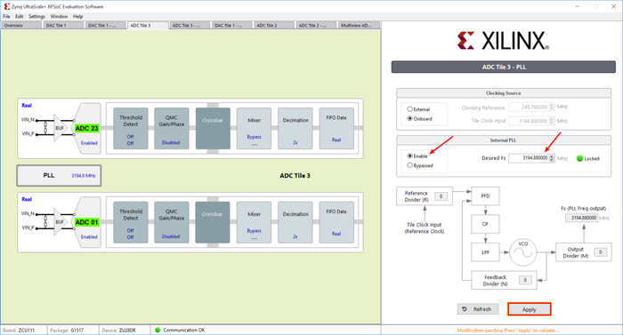
User should make sure the input clock rate is proper while using internal PLL enabled or when operating in bypass mode. When bypassing internal PLL, the input clock is sampling clock of converter, which is in general of the order of several GHz. On enabling internal PLL, the input clock is less than 1GHz. Please refer to RFSoC datasheet (DS926) for getting the proper frequencies both for using internal as well as external PLL.
Choose enable internal PLL as shown in the diagram and type the desired sampling frequency. Click on Apply.
Converter Settings
In each ADC/DAC tile, the available converter channels along with internal cascaded functional blocks are shown in block diagram. Clicking any functional block will show configuration page on the right panel.
...
FIFO
...
and
...
Crossbar
...
have their own separate pages.
ADC Settings
Calibration Mode: Indicates the optimized calibration mode based on signal location in the spectrum.
Nyquist Zone: Enables a user to choose which Nyquist zone the input signal should be located. This is related to interleaving calibration, should be indicated correctly. Zone 1 for odd and Zone 2 for even.
Threshold Detection: Sets embedded threshold detection parameter.
Decimation Settings: Allows a user to select the decimation factor. Don’t select
...
off
...
otherwise some digital blocks will be powered down and there won’t be any output.
DAC Settings
Decoder Mode: Enables a user to select between optimized noise floor or high linearity. Noise floor optimization should be chosen for communication application.
Nyquist Zone: Enables a user to choose which Nyquist zone the input signal should be located. This is related to interleaving calibration, should be indicated correctly. Zone 1 for odd and Zone 2 for even.
Interpolation Settings: Allows a user to select interpolation factor. Don’t select
...
off
...
otherwise some digital blocks will be powered down and there won’t be any output.
Inverse Sinc Settings: Enables Inverse Sinc to compensate sinc roll off at high frequency. This function is effective only when signal is in Nyquist zone 1.
...
Common settings
...
for ADC and DAC
Mixer Settings: Please set CrossBar page first, then set other parameters related to mixer and NCO.
QMC Settings: When enabling QMC block please set the gain, phase mismatch and offset mismatch.
FIFO Data Settings: Choose the number of words on AXI4S bus in PL side. Not currently supported.
FIFO: This page is only for information, no configurable settings currently available.
CrossBar Settings
Click
...
CrossBar
...
button at the bottom of converter settings page, or the
...
CrossBar
...
box in left diagram. This page determines the
...
Real
...
or
...
Complex
...
mode of Mixer and the multi-band configuration for Analog port.

FFT page
...
Clicking Acquisition
...
button in ADC settings page,
...
or Generation button in DAC settings page, will open the FFT page.
In DAC FFT page, single tone and dual tone generator is embedded in the UI. To generate complex modulated signal, user can load test vectors from a file.
There are variations of sub-menus in this page, including signal characteristics, customizing FFT plot, windowing function, test vector input and output etc. Refer to ADC FFT page as displayed below.

| Info |
|---|
...
For ADC FFT Analysis Max Hold is enabled by Default. Max Hold mode retains information of previous acquisition. |
Major functions and sub-menus in FFT page.

...
| Info |
|---|
Introduction of window function will cause some performance value degradation and this will |
...
NOT |
...
be compensated in this software. Please take this in to consideration when evaluating ADC performance. For example, NSD will degrade around 2dB when you introduce a window function. |
Hardware and Software Design Flow
Building the RFdc Hardware Design
Refer to
...
the Vivado Design Suite User Guide: Using the Vivado IDE, UG893, for setting up Vivado environment.
To build the hardware design, execute the following steps:
On Windows:
- Open a Vivado Tool.
- Navigate to the Eval Tool Folder Path and Change Directory to /pl folder.
- On the Tcl Console of the tool, type
source ./scripts/create_project.tcl
On Linux:
Please set $DCET_HOME environment variable as given below for linux environment
| Code Block |
|---|
% export DCET_HOME=</path/to/download/zipfile>/rdf0476-zcu111-RFdc-eval-tool-2018-3 |
1. Open a Linux terminal.
2. Change directory to $DCET_HOME/pl
3. There are three packages in the PL folder, user has to change directory accordingly.
4. To create the Vivado IPI project and invoke the UI, run the following command.
| Code Block |
|---|
% vivado -source scripts/create_project.tcl
|
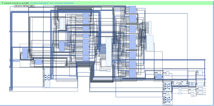
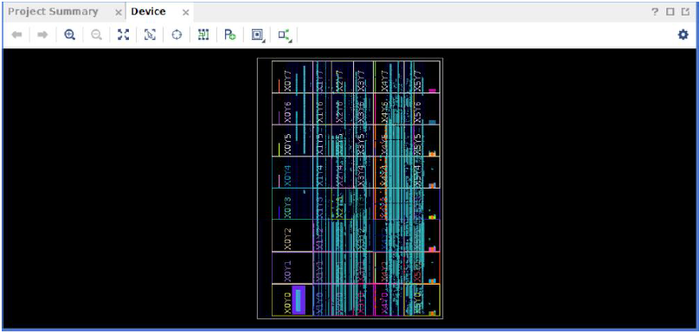
After executing the script on windows/linux systems, the vivado IPI block design comes up as shown in the following figure.
5. Click the "Generate Bitstream" on left hand side of Vivado Project Panel.
| Info |
|---|
...
If the user gets any pop-up with "No implementation Results available". Click "Yes". Then, if any pop-up comes up with "Launch runs", Click "OK". |
The design is implemented, and a pop-up window comes up saying "Open Implemented Design". Click "OK".
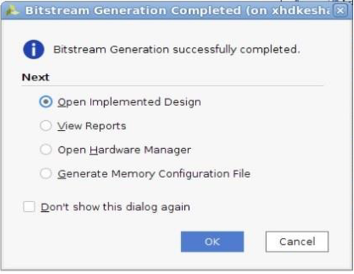
Below figure depicts the view of opened implemented design.
...
| Info |
|---|
The actual results might graphically look different than the image shown. |
6. Go to
...
File > Export > Export Hardware
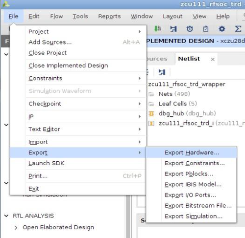
7. In the Export Hardware Platform for SDK window select "Include bitstream" and click "OK".
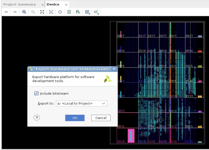
The XSA is created at $DCET_HOME/pl/project/zcu111_rfsoc_trd.sdk/zcu111_rfsoc_trd_wrapper.xsa
...
Building the PetaLinux Project
...
Exporting Hardware in 2020.1
- From the Vivado toolbar, select File → Export → Export Hardware.The Export Hardware dialog box opens.
- Choose Fixed and click Next.
- Choose Include device image and click Next.
- Provide the name for your exported file and choose the location. Click Next.
- A warning message appears if a Hardware Module has already been exported. Click Yes to overwrite the existing XSA file, if the overwrite message is displayed.Click Finis
Building the PetaLinux Project
| Info |
|---|
...
Refer to the PetaLinux Tool Documentation (UG1144) for installation.
Set $DCET_HOME environment variable as given below.
| Code Block |
|---|
% export DCET_HOME=</path/to/download/zipfile>/rdf0476-zcu111-RFdc-eval-tool-2018-3 |
1. Sourcing petalinux tool.
| Code Block |
|---|
% source <path/to/petalinux-installer>Petalinux-v2018.3/petalinux-v2018.3-final/settings.sh |
2. Post petalinux installation, $PETALINUX variable should be set, command to cross-check the variable.
| Code Block |
|---|
% echo $PETALINUX |
3. Create project from .bsp file
| Code Block |
|---|
% cd $DCET_HOME/apu/
% petalinux-create -t project -s rfsoc_petalinux_bsp.bsp
% cd rfsoc_petalinux_bsp |
| Info |
|---|
...
After creating project, please refer |
...
to Modifications on top of 2018.3 released BSP section, for detailed information on changes in this TRD on top of released 2018.3 |
...
PetaLinux BSP. |
4. Configure the PetaLinux project using step “a” or “b”.
a) with the pre-built xsa located in folder <pl/<design_path>pre-built/rfsoc_trd>, depending on the design user can select the "path". Make sure here the design_path indicates the folder in which the design/xsa resides.
| Code Block |
|---|
% petalinux-config --get-hw-description=$DCET_HOME/pl/<design_path>/pre-built/rfsoc_trd/ |
For Example : If the user wants to build for Non-MTS Design, the design_path would be similar to the one given in red ink.
| Code Block |
|---|
% petalinux-config --get-hw-description=$DCET_HOME/pl/NON-MTSDesign_8x8/project/zcu111_rfsoc_trd.sdk/ |
b) If Vivado project is modified/design is changed, user is expected to configure the bsp with the modified .xsa file.
| Code Block |
|---|
% petalinux-config --get-hw-description=$DCET_HOME/pl/<design_path>/project/zcu111_rfsoc_trd.sdk/ |
...
| Info |
|---|
After executing "petalinux-config" command, a prompt will be displayed . |
...
There is no need to change anything, Select "Exit" and come out of window. |
5. Build all Linux image components along with Evaluation Tool application
a) To build with SSR IP design replace system-user.dtsi and build
| Code Block |
|---|
% cp project-spec/meta-user/recipes-bsp/device-tree/files/system-user_ssr.dtsi project-spec/meta-user/recipes-bsp/device-tree/files/system-user.dtsi
% petalinux-build
|
b) To build with NON-MTS/MTS design replace system-user.dtsi and build
| Code Block |
|---|
% cp project-spec/meta-user/recipes-bsp/device-tree/files/system-user_8x8.dtsi project-spec/meta-user/recipes-bsp/device-tree/files/system-user.dtsi
% petalinux-build |
6. Create a boot image (BOOT.BIN) including FSBL, ATF, PMUFW, bitstream and u-boot.
| Code Block |
|---|
% cd images/linux
% petalinux-package --force --boot --fsbl zynqmp_fsbl.elf --fpga system.bit --pmufw pmufw.elf --u-boot u-boot.elf |
7. copy the BOOT.bin and image.ub to the sdcard.
| Code Block |
|---|
% cp BOOT.BIN image.ub $DCET_HOME/images/rev-B |
Modifications on top of 2018.3 released BSP
Below are the modification in this TRD for linux-kernel, rfdc drivers, rftool and rfdc example application, on top of 2018.3 petalinux released BSP.
For more details on patch information please refer to
...
...
...
A high level description is given below
...
:
- Kernel patch information as follows.
Code Block vi project-spec/meta-user/recipes-kernel/linux/linux-xlnx_%.bbappend SRC_URI_append = " \ file://0001-power-supply-irps-Add-support-for-irps-supply.patch \ file://0002-drivers-misc-add-support-for-DDR-memory-management.patch \ file://0003-dmaengine-xilinx_dma-In-SG-cyclic-mode-allow-multipl.patch \ file://0004-drivers-misc-add-support-for-selecting-mem-type.patch \ file://0005-i2c-cadence-Implement-timeout.patch \ file://0006-i2c-muxes-update-Mux-register-always.patch \ file://0007-drivers-misc-change-ADC-packet-size-as-per-FIFO-size.patch \ “ - RFDC driver patch information as follows.
Code Block vi project-spec/meta-user/recipes-bsp/rfdc/rfdc_%.bbappend SRC_URI_append = " \ file://0001-rfdc-add-support-to-turn-off-mixer.patch \ " Device tree patch information as follows.
Code Block vi project-spec/meta-user/recipes-bsp/device-tree/device-tree.bbappend SRC_URI_append = " \ file://0001-Fix-the-misc-clock-frequency-type.patch \ "RFTOOL application patch as follows.
Code Block vi project-spec/meta-user/recipes-apps/rftool/rftool.bbRFDC example application patch as follows.
Code Block vi project-spec/meta-user/recipes-apps/rfdc-data-write-example/rfdc-data-write-example.bb
RFDC Self-test application changes as follows.
Code Block vi project-spec/meta-user/recipes-bsp/rfdc-examples/rfdc-selftest_%.bbappend SRC_URI_append = " \ file://0001-examples-change-lmx-frequency-to-245Mhz.patch \ "
| Info |
|---|
...
To get "project-spec/meta-user/" folder, please extract files from. bsp using step #3 from section Building the PetaLinux Project. |
Appendix A Clock Switching Details
Appendix A.1 Internal PLL to External PLL
By default, System is booted with Internal PLL enabled and external PLL Bypassed. Please follow below mentioned steps and corresponding UI Snapshot to enable External PLL.
1) Internal PLL is enabled by default.

2) Select and click on Clock Settings.
3) Set ADC and DAC Clock. To maintain coherency set ADC/DAC as an integer multiple for example,ADC and DAC clocks are set to 3932.16 MHz to maintain coherency for loopback testing.
4) After changing the clock setting , the API will return failure.
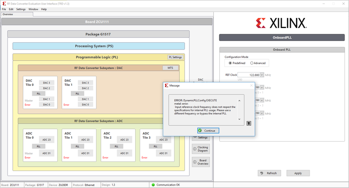 Note: -
| Info |
|---|
This a valid warning in the command window, as the design has currently internal PLL alive and the selected frequency in previous slide is out of the spec. of internal PLL. The user must press continue button and move on. |
5) Click on DAC tab and below screen will come up, Click on PLL
6) Select ‘Bypassed’ radio button and press Apply.
...
10) Click on PLL Button and Select Bypass Radio Button.
11) Repeat the same process for remaining ADC Tile 1,2,3.
12) Finally, all Internal PLLs will be bypassed as shown in below snapshot.
Appendix A.2 External PLL to Internal PLL
To revert to internal PLL, a user needs to set External PLL to a frequency which is required to enable internal PLL. In this design, Internal PLL reference clock is set to 245.76 MHz.
...
2) Set 245.76 for all LMX PLLs.

3) On the DAC Tile, Select PLL and Select Enable Radio Button.
...
6) Finally on the dashboard all Internal PLL will be enabled and shown in Green.
Appendix A.3 Advanced clock
This section describes the procedure for the user to use the Advanced clock for sampling all the DAC’s and ADC’s.
...
4) This tab has 4 options
- REF Clk - > LMK04208 PLL
- RFPLL 1 -> LMX2594 A
- RFPLL 2 -> LMX2594 B
- RFPLL 3 -> LMX2594 C
The user must set the frequencies by choosing the TCS files for each of the PLL’s. The RFPLL’s 1 and 2 are the sampling clocks for ADC’s and the RFPLL 3 is the sampling clock for DAC.
5) For example, the following frequencies have been chosen for all the PLL’s as shown in the figure below.
- REF Clk -> 122.88 MHz
- RFPLL 1 -> 3932.16 MHz
- RFPLL 2 -> 3932.16 MHz
- RFPLL 3 -> 3932.16 MHz
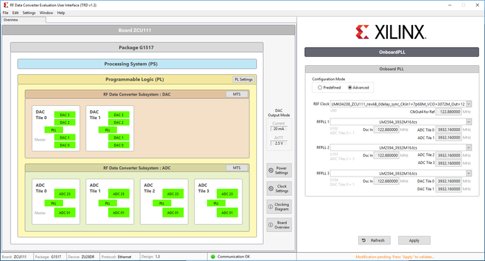
6) Press Apply
7) The user must now bypass the internal PLL for all DAC’s and ADC’s. Please refer to Appendix A.1 Internal PLL to External PLLfor steps to bypass Internal PLL and go to External PLL.
8) The sampling frequencies for all DAC’s and ADC’s have been set.
Appendix B Switching between memory types
By default, the UI is in BRAM mode. The steps to change the memory type between BRAM and DDR mode are as follows:
1) Click onPL Settingsbutton in the Overview tab on the UI.
2) By default, it is in BRAM mode. Please note BRAM has memory limitation of 128 KB only.
3) Choose DDR option from the dropdown menu. Press Apply. This will change the memory type from BRAM to DDR.
...
5) The UI is now in DDR mode. Choose BRAM option from the drop-down menu. Press Apply. This will change the memory type from DDR to BRAM.
| Info |
|---|
...
The user must regenerate and re-apply any DAC/ADC configuration when switched between BRAM and DDR modes. Not doing so will lead to spurious outputs. |
Appendix C Multiple channel support in DDR mode
The following steps show an example test for running the design for higher configuration in DDR mode.
...
4) Choose the DAC channels.Note:
| Info |
|---|
The user must make sure that the sampling frequency is set according to the table |
...
in Appendix A Performance Table of "ZCU111 RFSoC RF Data Converter Evaluation Tool Getting Started Guide" |
...
and same sample size is chosen for all channels. The test must be run in Multiview mode only. |
In this figure, the 4 channels of DAC Tile 1 have been chosen as an example.
5) Click on Generate All.
...
7) Choose the ADC channels.Note:
| Info |
|---|
User must make sure that the sampling frequency is set according to the table in and same sample size is selected for all channels. The test must be run in Multiview mode only. |
In the following figure, 2 channels from ADC Tile 1 and 2 channels from Tile 2 have been selected.
8) To acquire the DAC generated data in loopback mode, click on Acquire All.
Appendix D Dynamic Bitstream
In 2019.1 release of Eval tool a new feature has been added which lets the user switch between three Bitstreams dynamically. To exercise this feature the user needs to copy the following contents into the SD card
- mts folder
- nonmts folder
- ssr folder
- BOOT.bin
- image.ub
- autostart.sh
The following are the contents of the SD card package:
- mts -> contains BIN file and dt corresponding to the mts design
- nonmts -> contains BIN file and dt corresponding to the non_mts design
- ssr-> contains BIN file and dt corresponding to the ssr_ip design
- BOOT.bin,image.ub and autostart.sh -> images corresponding to the Eval Tool
The following section explains the steps to dynamically change the Bitstream using Eval Tool GUI.
...
Step 2: The bitstream type section allows the user to choose the bitstream.Note:
| Info |
|---|
By default the Eval tool comes up with NON_MTS Bitstream |
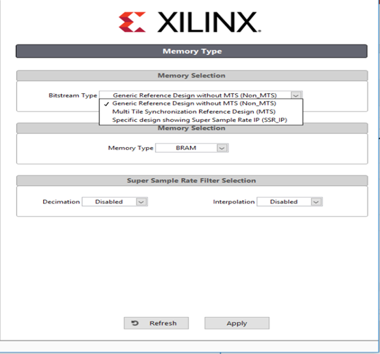
Step 3 : Once the user selects the Bitstream click on Apply. This will change the bitstream to the selected one.
...