MTS Design (8x8)
In the 2018.2 version of the design, all the features were the part of a single monolithic design. In the subsequent version the design has been split into three example designs based on the functionality. This section describes 8x8 (8-DAC, 8-ADC) channel MTS design. This example design is meant to demonstrate the Multi-Tile Sync (MTS) functionality of RFDC IP.
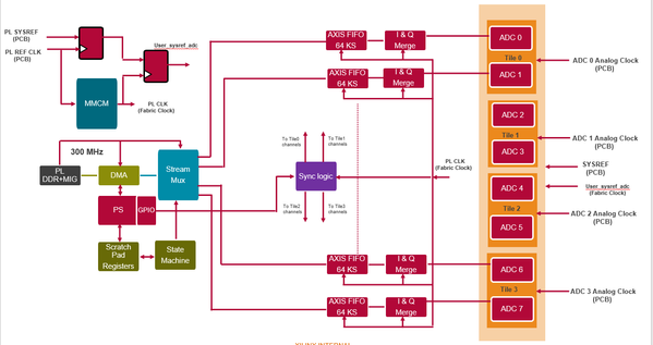
The data path for MTS design remains almost similar to that of the 2018.2 version of the monolithic design except for the reduced buffer sizes and simplification of clocking structure.
The contents of this page are as mentioned below.
Clocking and Control
The Clock Mux (BUFGMUXs) which is present in 2018.2 design for muxing MTS and Non-MTS clocks are not present in subsequent designs. The MTS design is clocked with PL clock as shown in the figure below. To further simplify the MTS design there is a common trigger signal for all channels rather than having individual trigger for all 8-channels on DAC and ADC sides. These triggers are enabled by using channel control GPIO pins. Also the GPIO required to differentiate between Non MTS and MTS design is no longer required. The corresponding constraints for GPIOs and clock structure have also been modified. The updated constraint files are provided as the part of the TRD ZIP Package.
For DAC

For ADC
RFSoC RFdc Build and Run Flow Tutorial
The following link will navigate the user to the RFSoC RFdc Build and Run Flow Tutorial page for further details.
Multi-tile Synchronization (MTS) Run Flow
- Open the RF_DC_Evaluation_UI.ini file from the UI Installation path and add the following
[Display]
ShowMTS = TRUE
EnableAdvancedClocking = True
ShowExtClock = True
This will enable MTS, Advanced Clocking settings in UI.
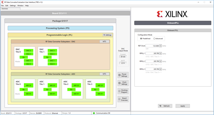
2. The UI Overview window is as shown in the following figure. By default, MTS is not enabled.
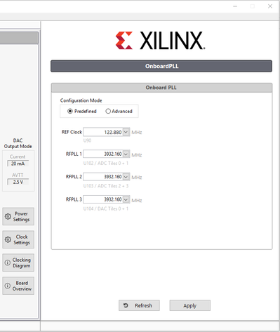
3. Click on the Clock Settings.
4. Set the RFPLL 1, RFPLL 2 and RFPLL 3 frequencies to 3932.16 MHz. Press Apply.
5. Once these frequencies are chosen,the user needs to bypass the Internal PLL for all the DAC’s and ADC’s. Refer to Appendix A.1 Internal PLL to External PLL of the (RFSoC Build and Run Flow Tutorial) for steps to bypass Internal PLL and go to External PLL.
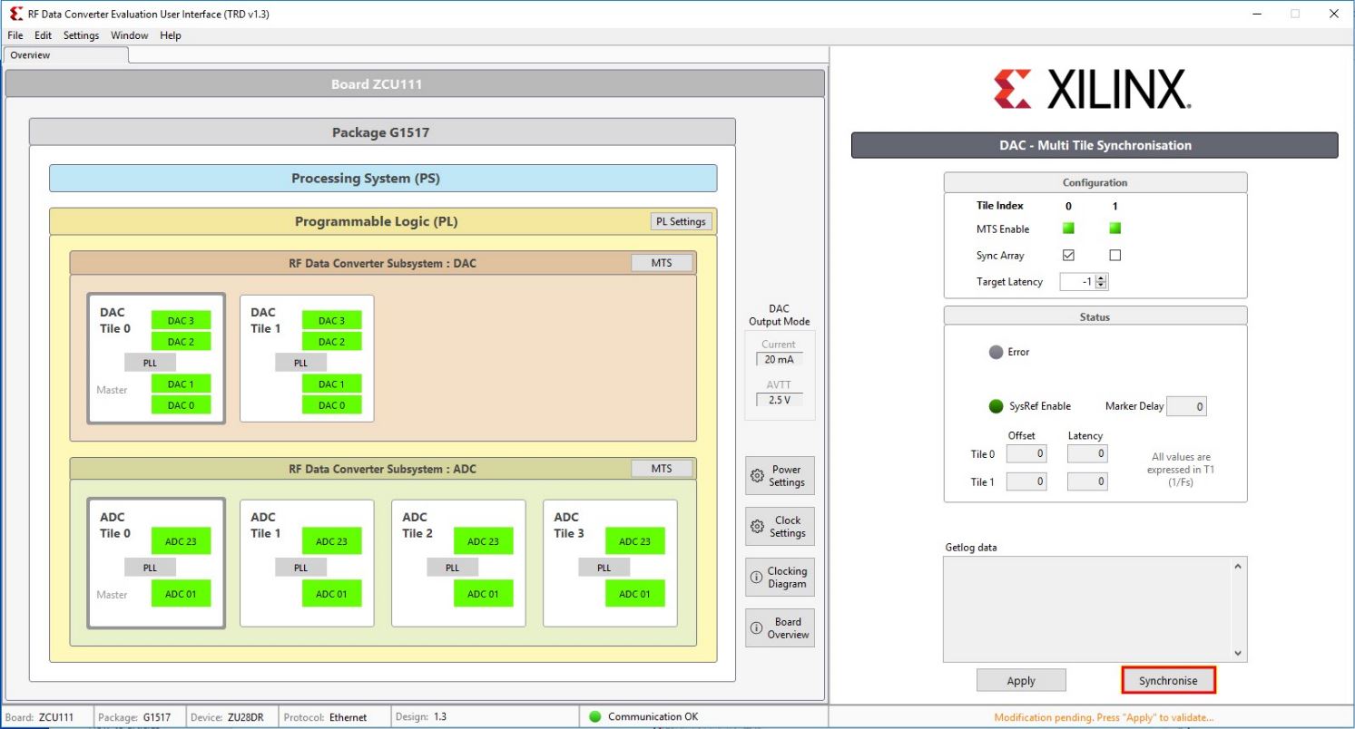
6. Once the PLL’s are bypassed, the user needs to enable MTS. Click on MTS button of DAC in the Overview tab of the UI.
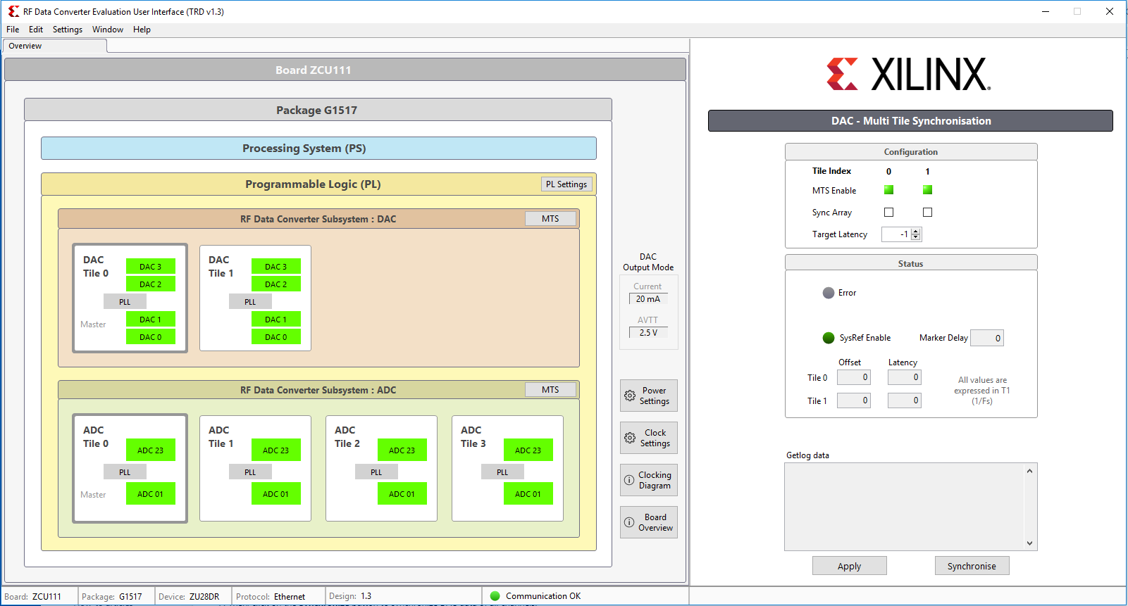
7. Enable MTS by clicking on the checkbox and press Apply.

8. Then, click on the Synchronize button.
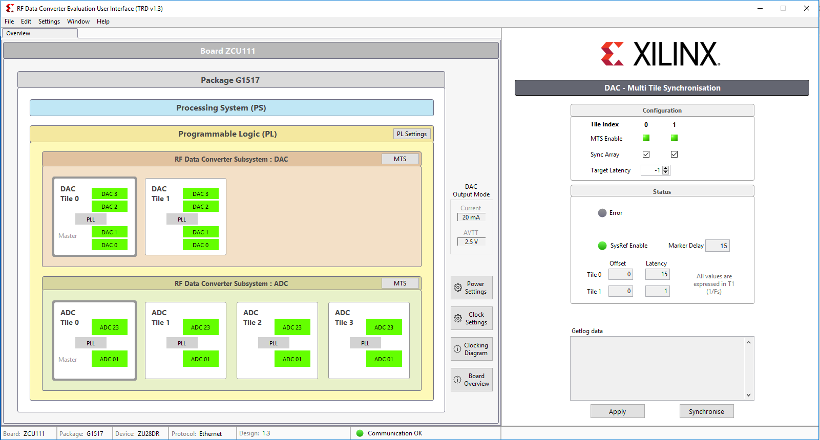
9. The MTS window looks as shown in the figure below after synchronization.
10. Click on the MTS button of ADC in the Overview tab of the UI.
11. Enable the MTS by clicking on the checkbox and press Apply.

12. Then, click on Synchronize button.

13. The MTS window looks as shown in the figure below after synchronization.

14. Go to Window -> Multiview -> DAC FFT.
15. Select all DAC channels sequentially as shown in the following figure.
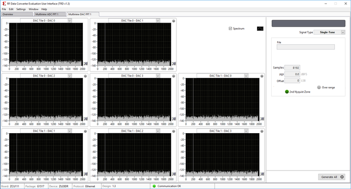
16. Once all the DAC channels are chosen, clock on the Generate All button. This will generate data on all DAC channels.
17. Go to Window -> Multiview -> ADC Time Domain.
18. Select all the ADC channels as shown in the figure below.

19. Once all the channels are selected, click on the Acquire button. The output looks as shown in the figure below. All the ADC channels will be in a synchronization.

Note: On the first acquisition, the data might not appear to be in sync. On successive acquisitions, the data will be in sync.
Note:1) The MTS test must be performed in BRAM mode and Multiview window only.
2) When the user changes any configuration setting of DAC/ADC, they must apply those settings but the generation and acquisition must be done in Multiview window only.
3) Once the MTS test is run, to re-run it again, the user must do the following:
▪ Disable MTS for both DAC and ADC
▪ Enable MTS for both DAC and ADC.
▪ Synchronize
▪ Generate and Acquire in Multiview window
4) If interleaved spurs are noticed in ADC FFT plot, user must toggle the calibration mode of the corresponding ADC channel.
Make sure Cal. Free button is Un-Checked before toggling the modes.
Once this step is done, repeat step 3. Not following any of the above steps will lead to spurious outputs.
GPIO List
| DAC | ADC | Common | |||
|---|---|---|---|---|---|
| Function | GPIO# | Function | GPIO# | Function | GPIO# |
| DAC0 Reset | 0 | ADC0001 Reset | 32 | DAC_3to8_Decoder_sel | 67:64 |
| DAC0 Loopback select | 1 | ADC0001_IQ_Merge_sel | 33 | ||
| DAC0 BW Monitor enable | 69 | ||||
| DAC0 Future Use | 3 | ADC0001 Future Use | 35 | DAC1 BW Monitor enable | 70 |
| DAC1 Reset | 4 | ADC0203 Reset | 36 | Future Use | 79:71 |
| DAC1 Loopback select | 5 | ADC0203_IQ_Merge_sel | 37 | ADC Channel Mux sel | 82:80 |
| Future Use | 83 | ||||
| DAC1 Future Use | 7 | ADC0203 Future Use | 39 | ||
| DAC2 Reset | 8 | ADC1011 Reset | 40 | Future Use | 94:85 |
| DAC2 Loopback select | 9 | ADC1011_IQ_Merge_sel | 41 | ||
| DAC2 Future Use | 11 | ADC1011 Future Use | 43 | ||
| DAC3 Reset | 12 | ADC1213 Reset | 44 | ||
| DAC3 Loopback select | 13 | ADC1213_IQ_Merge_sel | 45 | ||
| DAC3 Future Use | 15 | ADC1213 Future Use | 47 | ||
| DAC4 Reset | 16 | ADC2021 Reset | 48 | ||
| DAC4 Loopback select | 17 | ADC2021_IQ_Merge_sel | 49 | ||
| DAC4 Future Use | 19 | ADC2021 Future Use | 51 | ||
| DAC5 Reset | 20 | ADC2223 Reset | 52 | ||
| DAC5 Loopback select | 21 | ADC2223_IQ_Merge_sel | 53 | ||
| DAC5 Future Use | 23 | ADC2223 Future Use | 55 | ||
| DAC6 Reset | 24 | ADC3031 Reset | 56 | ||
| DAC6 Loopback select | 25 | ADC3031_IQ_Merge_sel | 57 | ||
| DAC6 Future Use | 27 | ADC3031 Future Use | 59 | ||
| DAC7 Reset | 28 | ADC3132 Reset | 60 | ||
| DAC7 Loopback select | 29 | ADC3132_IQ_Merge_sel | 61 | ||
| DAC7 Future Use | 31 | ADC3132 Future Use | 63 | ||
© Copyright 2019 - 2022 Xilinx Inc. Privacy Policy