Non-MTS Design (8x8)
In the 2018.2 version of the design, all the features were part of a single monolithic design. In the subsequent version the design has been split into three example designs based on the functionality (MTS only design, Non MTS design and SSR IP design). This section describes 8x8 (8-DAC, 8-ADC) channel Non-MTS design. This example design demonstrates most of the features of RFDC IP except for Multi-Tile Sync (MTS).
The data path for Non-MTS design remains almost similar to that of the 2018.2 version of monolithic design except for the reduced buffer sizes and simplification of clocking structure.
The contents of this page are as mentioned below.
New Feature Addition
In 2018.2 version of design the data was captured sequentially for all the ADC based on the GUI request that itself came sequentially. In the subsequent version data is simultaneously captured for all the 8-ADC channels and provided to GUI sequentially. This now enables the user to simultaneously capture very large sample sizes by making use of large DDR storage.The performance numbers related to DAC/ADC is published on Performance Tables Appendix A Performance Table (of the ZCU111 RFSoC RF Data Converter Evaluation Tool Getting Started Guide).
Clock and Control Changes
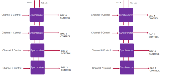
The design is clocked with the respective DAC and ADC clocks. There is no usage of PL Clock/SysRef clock in non MTS Mode. Hence the Clock Muxes (BUFGMUXs) have been removed from the design. The channels are clocked using clocks derived from their respective tiles and not from a common source as is the case in MTS design. This design has individual channel start/trigger signals and the common channel start/trigger signal required for MTS is removed. Hence the corresponding GPIO is also removed. The updated design constraint file is updated as a part of the Non-MTS design example design package.
The following is the block diagram of the Non MTS design (DAC side),Corresponding changes are there on ADC side also.
For DAC

For ADC

Non-MTS GPIO Control
RFSoC RFdc Build and Run Flow Tutorial
The following link will navigate the user to the RFSoC RFdc Build and Run Flow Tutorial page page for further details.
Non-MTS Run Flow
Set up the following parameter in the UI as shown below and follow the instructions as mentioned in this section.
DAC Configuration
DAC- Fs (Sampling frequency) = 6389.76 MHz
CF (Centre frequency) = 200 MHz (DAC0), 150 MHz (DAC1)
Nsamples (Number of samples) = 8192
Interpolation =8x, IQ to Real
Fine Mixer Frequency = 1500 MHz
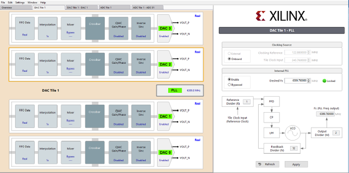
Double click the DAC Tile.
Change the DAC internal PLL frequency to 6389.76 MHz as shown in figure below. Press Apply once all the frequencies are chosen. These PLL clock frequencies are the sampling frequencies for the DAC’s and ADC’s.
1. Click the DAC 0 block. The various configuration settings can be seen on the page. Change the settings to IQ mode from Real mode by clicking the Crossbar button of the corresponding DAC channel. Set the other configurations as shown in the figure below. Click the Apply button.

2. Once the settings are completed, click on the Generation button. This tab has the FFT and Raw data display for DAC 0. Enter the CF and number of Samples. Click on the Generate button to generate the waveform.

3. Click on the DAC 1 block. The various configuration settings can be seen in the page. Change the settings to IQ mode from Real mode by clicking the Crossbar button of the corresponding DAC. Set the other configurations as shown in the figure below. Click on the Apply button.
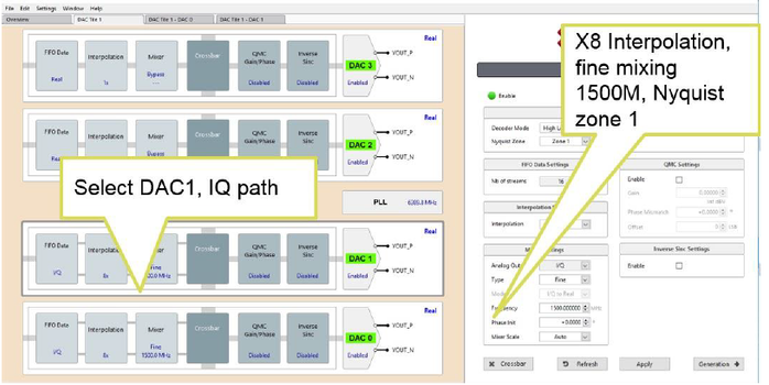
4. Once the settings are completed, click on the Generation button. This tab has the FFT and Raw data display of the DAC 1 channel. Enter the CF and number of Samples. Click on the Generate button to generate the waveform.

ADC Configuration
ADC- Fs = 3194.88 MHz
Nsamples = 8192
Decimation = 4x
Cal Mode = 2
Fine Mixer Frequency = -1200 MHz (To Test Complex Lower Sideband)
1. Double click on the ADC Tile. Change the ADC internal PLL frequency to 3194.88 MHz.
2. Click on the ADC 01 block. The various configuration settings can be seen. By default, it is in IQ mode. Set the other configurations as shown in the figure below. Click the Apply button.

3. Once the settings are completed, click on the Acquisition button. This tab has the FFT and Raw data display of the ADC 01 data. Enter the number of Samples. Click on the Acquire button, the FFT plot is displayed.
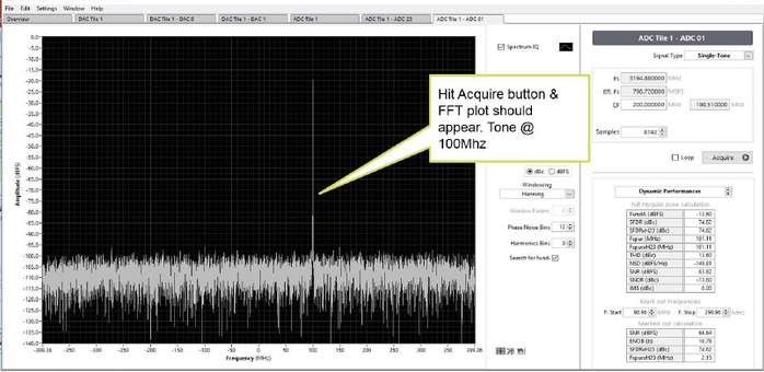
4. Click on the ADC 23 block. The various configuration settings can be seen on the page. By default, it is in IQ mode. Set the other configurations as shown for ADC 01. Click on the Apply button.
5. Once the settings are completed, click on the Acquisition button. This tab has the FFT and Raw data display of the ADC 23 channel. Enter the number of Samples. Click on the Acquire button, the FFT plot is displayed.
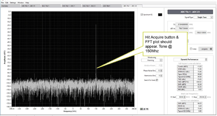 Note: Windowing might be needed to make a coherent setup to clean up the FFT plot. Hanning window is a good selection.
6. The user can enable the ADC looping function to emulate a real time spectrum analyzer. Check on the loop checkbox and click on the Acquire button.
For more relevant information please refer to the following sections.
- Appendix A Clock Switching Details of the RFSoC Build and Run Flow Tutorial.
- Appendix B Switching between memory types of the RFSoC Build and Run Flow Tutorial.
- Appendix C Multiple channel support in DDR mode of the RFSoC Build and Run Flow Tutorial.
GPIO List
| DAC | ADC | Common | |||
|---|---|---|---|---|---|
| Function | GPIO# | Function | GPIO# | Function | GPIO# |
| DAC0 Reset | 0 | ADC0001 Reset | 32 | DAC_3to8_Decoder_sel | 67:64 |
| DAC0 Loopback select | 1 | ADC0001_IQ_Merge_sel | 33 | ||
| DAC0 local start | 2 | ADC0001001 local start | 34 | DAC0 BW Monitor enable | 69 |
| DAC0 Future Use | 3 | ADC0001 Future Use | 35 | DAC1 BW Monitor enable | 70 |
| DAC1 Reset | 4 | ADC0203 Reset | 36 | Future Use | 79:71 |
| DAC1 Loopback select | 5 | ADC0203_IQ_Merge_sel | 37 | ADC Channel Mux sel | 82:80 |
| DAC1 local start | 6 | ADC0203 local start | 38 | Future Use | 83 |
| DAC1 Future Use | 7 | ADC0203 Future Use | 39 | ||
| DAC2 Reset | 8 | ADC1011 Reset | 40 | Future Use | 94:85 |
| DAC2 Loopback select | 9 | ADC1011_IQ_Merge_sel | 41 | ||
| DAC2 local start | 10 | ADC1011 local start | 42 | ||
| DAC2 Future Use | 11 | ADC1011 Future Use | 43 | ||
| DAC3 Reset | 12 | ADC1213 Reset | 44 | ||
| DAC3 Loopback select | 13 | ADC1213_IQ_Merge_sel | 45 | ||
| DAC3 local start | 14 | ADC1213 local start | 46 | ||
| DAC3 Future Use | 15 | ADC1213 Future Use | 47 | ||
| DAC4 Reset | 16 | ADC2021 Reset | 48 | ||
| DAC4 Loopback select | 17 | ADC2021_IQ_Merge_sel | 49 | ||
| DAC4 local start | 18 | ADC2021 local start | 50 | ||
| DAC4 Future Use | 19 | ADC2021 Future Use | 51 | ||
| DAC5 Reset | 20 | ADC2223 Reset | 52 | ||
| DAC5 Loopback select | 21 | ADC2223_IQ_Merge_sel | 53 | ||
| DAC5 local start | 22 | ADC2223 local start | 54 | ||
| DAC5 Future Use | 23 | ADC2223 Future Use | 55 | ||
| DAC6 Reset | 24 | ADC3031 Reset | 56 | ||
| DAC6 Loopback select | 25 | ADC3031_IQ_Merge_sel | 57 | ||
| DAC6 local start | 26 | ADC3031 local start | 58 | ||
| DAC6 Future Use | 27 | ADC3031 Future Use | 59 | ||
| DAC7 Reset | 28 | ADC3132 Reset | 60 | ||
| DAC7 Loopback select | 29 | ADC3132_IQ_Merge_sel | 61 | ||
| DAC7 local start | 30 | ADC3132 local start | 62 | ||
| DAC7 Future Use | 31 | ADC3132 Future Use | 63 | ||
© Copyright 2019 - 2022 Xilinx Inc. Privacy Policy