SSR IP Design (1x1)
This is a 1x1 (1-DAC, 1-ADC channels) design. In 2018.3 version of design update , a new feature is added in programmable logic (PL) portion of the design. In the Fabric, interpolation and decimation filters are added to DAC and ADC path respectively to showcase how easily PL based component can be added in RF Data path of the evaluation design.The fabric filters are generated using the newly introduced SysGen tool from Xilinx.
Detailed description is given in the sections below.
Introduction to SysGen Tool
The SysGen tool generates Filter IP in Vivado IPI block format so that they can be easily integrated into the existing design.
Procedure to Generate SSR IP via SysGen Flow
For more information on IP generation by system generator flow, refer the document online at https://www.xilinx.com/products/design-tools/vivado/integration/sysgen.html documentation.
- Open the SysGen from the command prompt and then open the corresponding interpolation/decimation filter from the TRD zip folder.
2. Click on the system generator token as shown in figure below.

3. On clicking the token, the tab opens as shown in figure below.

4. Click on generate to generate the IP.
Note:
- Coefficients for Interpolation and Decimation filter can be obtained from Coefficients for Interpolation page 76 and Coefficients for Decimation page 49 of PG 269.
- All filters are individually generated in IPI format.
- Once these filters are generated they can be integrated into the existing VIVADO design.
Integration of SSR IP into Vivado 2018.3/2019.1
To keep it simple the example design just instantiates one DAC and ADC channels and SSR IPs are added to the path as shown in the figure below.Overall 3 IPs of x2 configuration are generated. These IPs are connected in back to back format to achieve x8 Interpolation and x8 decimation. AXIS FIFO are added at each stage of filters for better timing closure. These filters can be enabled/disabled using the GPIO pins which are controlled via LabVIEW GUI.
The design for the x8 Interpolation using SSR IP is as shown in the figure below.
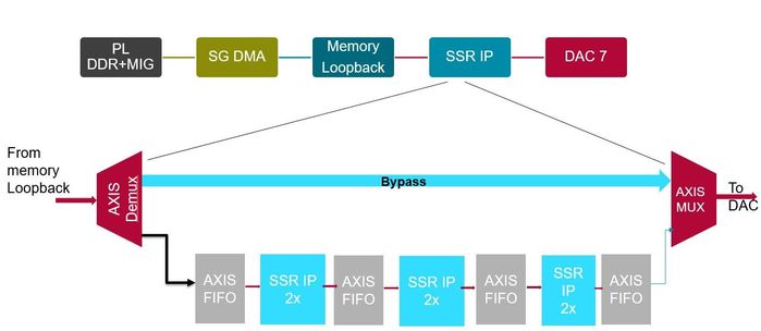
The design for the x8 decimation using SSR IP as as shown in the figure below.

RFSoC RFdc Build and Run Flow Tutorial
The Following link will navigate the user to the RFSoC RFdc Build and Run Flow Tutorial page for further details.
SSR IP functionality using the UI
- Open the UI.
- Click on "PL Settings" button.
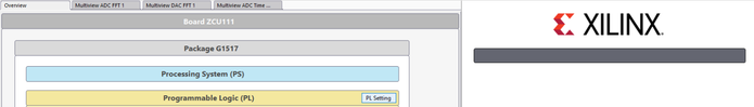
3. The user can see the memory selection and Super Sample Rate selection tabs.
4. Click on the drop-down option for Interpolation, select 8x and then click Apply.
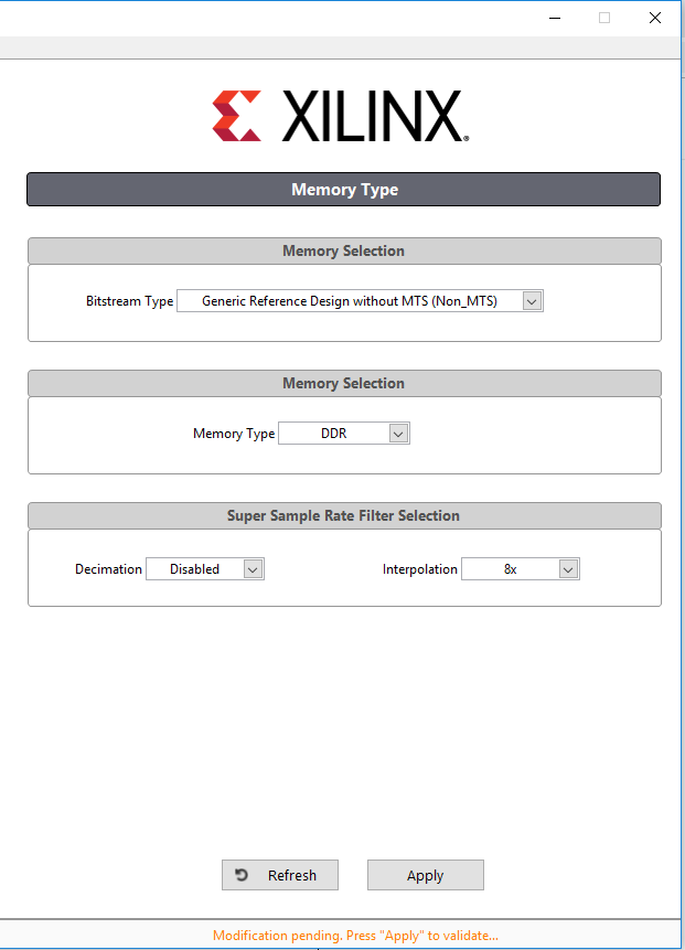
5. This will enable the PL interpolation filter.
6. Click on the drop-down option for decimation, select 8x and then click apply
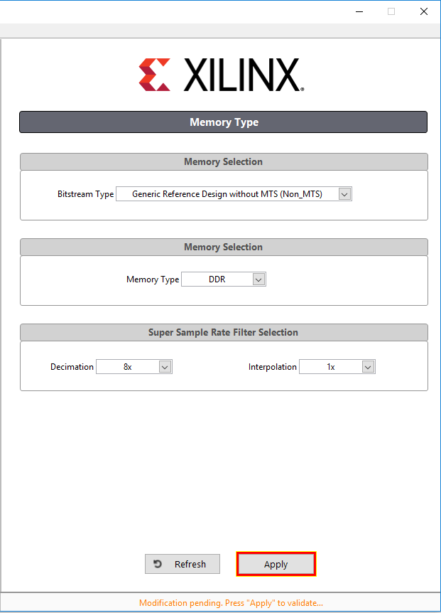
7. This will enable the PL decimation filter.
8. To bypass filter user needs to choose 1x for both interpolation and decimation and then press apply.
Following is the example for decimation x8 using SSR IP
DAC Fs= 3932.16 MHz
DAC CF= 200 MHz
Interpolation = x1
ADC Fs= 3932.16 MHz
Decimation= x8 (SSR)
The ADC output when the above settings are applied is as shown below:
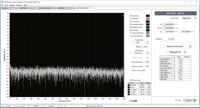
Note: The user is expected to see a decrease in output amplitude by ~25 db.
© Copyright 2019 - 2022 Xilinx Inc. Privacy Policy