Zynq PCIe TRD 14.4
Zynq PCIe TRD 14.4
Table of Contents
History
ISE DS 14.3 Zynq PCIe Targeted Reference Design
1 Introduction
This page provides instructions on how to build various components of the Zynq PCIe Targeted Reference Design (TRD) and how to setup the hardware platform and run the design on the ZC706 Evaluation Kit. The ZC706 Evaluation kit is based on a XC7Z045 FFG900-2 Zynq-7000 SoC device. For additional information, refer to UG961.
1.1 About the Zynq PCIe TRD
The Zynq PCIe Targeted reference design expands the Base Targeted Reference Design (UG925) by adding PCI Express communication with a host system at PCIe x4 GEN2 speed. In the Base Targeted Reference design, the input of the video processing pipeline is generated by a test pattern generator in the FPGA fabric. In this design, the input of the video processing pipeline is generated by an application on the host computer at 1080p60 resolution and transmitted to the ZC706 board via PCIe. The data is processed by video pipeline and passed back to the host system via PCIe. As full 1080p60 video stream only take up around 4Gbps, an additional data generator and a checker are implemented and connected to channel 1 of PCIe DMA showcasing the maximum PCIe x4 GEN2 bandwidth achieved by the hardware. For additional information, please refer to UG963

1.2 Zynq PCIe TRD Package Contents
The Zynq PCIe TRD package is released with the source code, Xilinx PlanAhead and SDK projects, and an SD card image that enables the user to run the video demonstration and software application. It also includes the binaries necessary to configure and boot the Zynq-7000 AP SoC board. The package also contains the software driver source files required to run application software in the PCIe host machine. This wiki page assumes the user has already downloaded the PCIe TRD package and extracted its contents to the PCIe TRD home directory referred to as ZYNQ_TRD_HOME in this wiki and to the PCIe host machine in a folder of choice.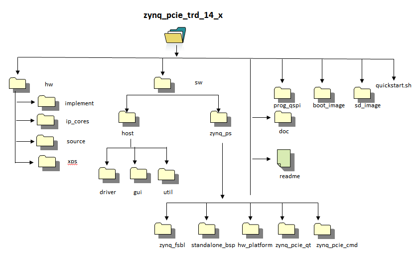
2 Prerequisites
- The ZC706 Evaluation Kit ships with the version 14.x Device-locked to the Zynq-7000 XC7Z045 FFG900-2 device and all required licenses to build the TRD. For additional information, refer to UG798 ISE Design Suite 14: Installation and Licensing Guide.
- PC with PCIe v2.0 slot. Recommended PCI Express Gen2 PC system motherboards are ASUS P5E (Intel X38), ASUS Rampage II Gene (Intel X58) and Intel DX58SO (Intel X58).
- Fedora 16 LiveCD for booting Linux on PCIe host machine.
- A Linux development PC with the ARM GNU tools installed. The ARM GNU tools are included with the Xilinx ISE Design Suite Embedded Edition or can be downloaded separately.
- A Linux development PC with the distributed version control system Git installed. For more information, refer to Using Git and to UG821: Xilinx Zynq-7000 EPP Software Developers Guide.
Tools Required
Tools for Software build
- Windows XP/Windows7
- SDK 14.4
For building Linux kernel and application of Zynq PS:
- ARM cross compile tool
- mkimage
- corkscrew
- git
- Open JDK
3 Building the FPGA Hardware Bitstream
This section explains how to generate the FPGA hardware bitsream using the Xilinx PlanAhead tool and how to export the hardware platform to Xilinx Software Development Kit (SDK) for software application development. Inside the PlanAhead project, a Xilinx Platform Studio (XPS) project is referenced that contains the embedded hardware design. The design top level file instantiates the embedded top level file along with the system with PCIe IP wrapper, PCIe DMA, PCIe performance monitor and hardware generator and checker blocks.
3.1 Building the Bitstream
A pre-compiled bitstream can be found at $ZYNQ_TRD_HOME/boot_image/z7_pcie_trd.bit.
Note: The TRD uses Tandem PROM flow to generate the bitstream.
Tandem PROM flow generates a two staged bitstream.
The first stage bitstream is smaller sized bitstream and is used to
meet 100 ms boot up time requirement in PCIe based End Points.
For more information, please refer to PG054,
7 Series FPGAs Integrated Block for PCI Express Product Guide
Browse to zynq_pcie_trd_14_4/hw/implement/plan_ahead directory:
- On Windows 7, on ISE Design Suite Command Prompt. Open ISE Design Suite Command Prompt by navigating Start > All Programs > Xilinx Design Tools 14.x > ISE Design Suite 14.x > Accessories. Run “launch_pa.bat” .
- On Linux, enter run ./launch_pa.sh at the command prompt.
In the Flow Navigator pane on the left-hand side under Program and Debug, click Generate Bitstream. The bitstream will be generated at $ZYNQ_TRD_HOME/hw/implement/plan_ahead/planAhead_run_1/z7_pcie_trd.runs/impl_1/z7_pcie_trd.bit.
- Note: Click on Save button when prompted for Save Project Before Generating Bitstream

Note: A message window will pop up, saying there are critical warning messages. Ignore these warnings and press OK to continue with the bitstream generation.
3.2 Exporting the Hardware Platform to SDK: Building Drivers for Zynq PS
A pre-generated hardware platform project can be found at $ZYNQ_TRD_HOME/sw/zynq_ps/hw_platform.
Steps for exporting the hardware platform to SDK
From the PlanAhead project flow navigator click on Open Implemented Design. Click on "OK" when prompted for no trace timing results were found.. message
From the PlanAhead menu bar, select File > Export > Export Hardware.
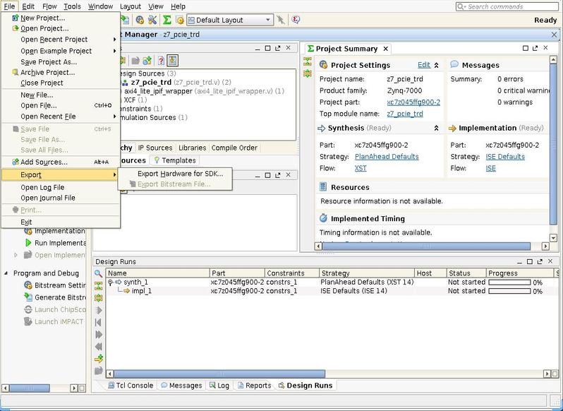
In the Export Hardware window press OK. The SDK hardware platform will be exported to $ZYNQ_TRD_HOME/hw/implement/plan_ahead/planAhead_run_1/z7_pcie_trd.sdk/SDK/SDK_Export.
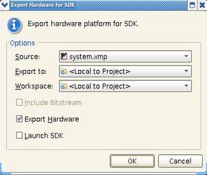
Note: If the Launch SDK option is checked in the Export Hardware window, SDK will be launched immediately after SDK export has completed. This is not recommended at this point.
4 Building the First Stage Boot Loader (FSBL)
This section explains how to import and build the First Stage Boot Loader (FSBL) and the standalone OS based Board Support Package (BSP) from the provided SDK projects. A pre-compiled FSBL executable can be found at $ZYNQ_TRD_HOME/boot_image/zynq_fsbl.elf.Note: The provided FSBL project is a customized version of the FSBL SDK project template. The following features have been added to the Zynq PCIe TRD version:- added I2C initialization sequence for HDMI transmitter (ADV7511) on ZC706 PCIe board
Steps for building the FSBL
Launch Xilinx SDK:- On Windows 7, select Start > All Programs > Xilinx Design Tools 14.x > ISE Design Suite 14.x > EDK > Xilinx Software Development Kit.
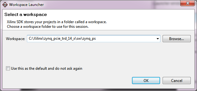
- On Linux, enter xsdk at the command prompt.In the Workspace Launcher window, click Browse and navigate to $ZYNQ_TRD_HOME/sw/zynq_ps, then click OK. Close the welcome screen.
To import the hardware platform (hw_platform) and FSBL (zynq_fsbl) SDK projects into the SDK workspace, select File > Import.

Note: The zynq_fsbl project requires a hardware platform SDK project generated by SDK export. Instead of the provided hw_platform project, the one generated in Section 3.2 can be used. This requires the user to update the project reference of the zynq_fsbl project. This is not recommended at this point.
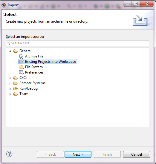
In the Import wizard, expand the General folder, select Existing Projects into Workspace, and click Next.
All projects are located at the top-level inside your SDK workspace. Click Browse and navigate to $ZYNQ_TRD_HOME/sw/zynq_ps. Press OK.

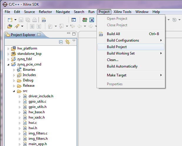
Make sure the hw_platform, standalone_bsp and zynq_fsbl projects are checked and uncheck the zynq_pcie_cmd and zynq_pcie_qt projects for now. Press Finish.

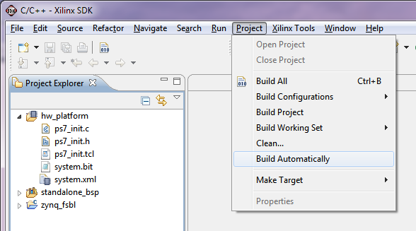
The build process will start automatically and builds the BSP first and then the FSBL. The generated Zynq FSBL executable can be found at $ZYNQ_TRD_HOME/sw/zynq_ps/zynq_fsbl/Debug/zynq_fsbl.elf. This option can be changed by unchecking Project > Build Automatically from the menu bar.
To manually build the project, right click zynq_fsbl in the Project Explorer and select Build Project; to clean the project, select Clean Project.

5 Building the U-boot Boot Loader
This section explains how to download the sources, configure, and build the U-boot boot loader for the Zynq PCIe TRD. A pre-compiled U-boot executable can be found at $ZYNQ_TRD_HOME/boot_image/u-boot.elf. For additional information, refer to the Xilinx Zynq U-boot wiki. This step requires a Linux development PC with the ARM GNU tools and Git installed (see Section 3.2 ).
Steps for building the U-boot boot loader
Set the CROSS_COMPILE environment variable and add it to your PATH.
bash> export CROSS_COMPILE=arm-xilinx-linux-gnueabi-
bash> export PATH=/path/to/cross/compiler/bin:$PATH
Clone the latest Zynq U-boot git repository from the Xilinx git server.
bash> cd $ZYNQ_TRD_HOME
bash> git clone git://github.com/Xilinx/u-boot-xlnx.git
Create a new branch named zynq_pcie_trd_14_4 based on the Xilinx-14.4-build2-trd tag. The Zynq PCIe TRD U-boot tag is built on top of the 14.4 release tag.
bash> cd $ZYNQ_TRD_HOME/u-boot-xlnx
bash> git checkout -b zynq_pcie_trd_14_4 xilinx-v14.4
Apply the PCIe TRD specific patch on top of the Zynq PCIe TRD tag. The patch includes:
- u-boot address modification for loading more than 16 MB of data into QSPI by changing 0xFC100000 ->0xFD000000, 0xFC600000->0xFD600000, FC800000->FD800000
bash> cp $ZYNQ_TRD_HOME/patches/zynq_pcie_trd_u-boot_14_4.patch . // copy the 14.4 TRD patch from package to dev PC
bash> git apply --stat zynq_pcie_trd_u-boot_14_4.patch    // display contents of patch
bash> git apply --check zynq_pcie_trd_u-boot_14_4.patch  // check if patch can be applied
bash> git am zynq_pcie_trd_u-boot_14_4.patch  // apply the patch
Configure U-boot for the Zynq ZC706 PCIe TRD.
bash> make zynq_zc70x_config
Build the U-boot boot loader. The generated U-boot executable can be found at $ZYNQ_TRD_HOME/u-boot-xlnx/u-boot.
bash> make
Rename this executable to u-boot.elf. This elf is used for generating BOOT image.
bash> mv u-boot u-boot.elf
6 Building the Boot Image
The TRD uses two boot images- BOOT.bin is used for SD boot mode in order to program the QSPI device with TRD boot image and kernel images. The zc706_pcie_trd.bin contains the TRD bitstream. This section explains how to create a boot image zc706_pcie_trd.bin from pre-compiled binaries provided in this package. The pre-compiled binaries are located at $ZYNQ_TRD_HOME/boot_image and include zynq_fsbl.elf, z7_pcie_trd.bit, and u-boot.elf. Alternatively, the user can use the generated files from Sections 3.1, 4, and 5. Pre-generated boot images can be found at $ZYNQ_TRD_HOME/prog_qspi/BOOT.bin and $ZYNQ_TRD_HOME/prog_qspi/zc706_pcie_trd.bin.
Steps for building the boot image
Launch Xilinx SDK:
- On Windows 7, select Start > All Programs > Xilinx Design Tools 14.x > ISE Design Suite 14.x > EDK > Xilinx Software Development Kit.
- On Linux, enter xsdk at the command prompt.
In the Workspace Launcher window, click Browse and navigate to $ZYNQ_TRD_HOME/sw/zynq_ps, then click OK.
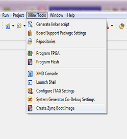
Select Xilinx Tools > Create Boot Image from the menu bar.
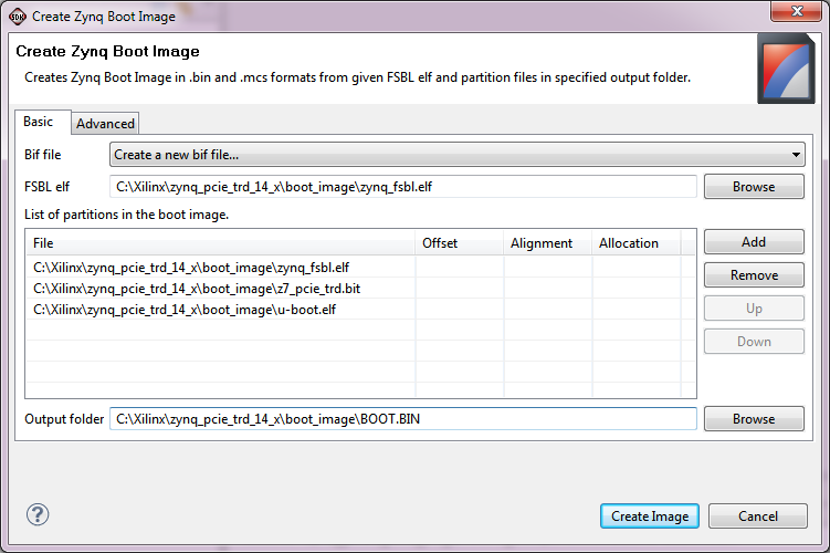
In the Create Zynq Boot Image dialog box, browse to select the FSBL elf file and add the files zynq_fsbl.elf, z7_pcie_trd.bit, and u-boot.elf from the $ZYNQ_TRD_HOME/boot_image directory and enter or browse to $ZYNQ_TRD_HOME/boot_image in the output folder field as shown in the figure. Press Create Image. This step will generate a file named under u-boot.bin, rename this to zc706_pcie_trd.bin at the specified location.
Notes:
- Occasionally, an internal error message pops up which can be safely ignored.
- The boot image has to be named zc706_pcie_trd.bin so the QSPI programming script init.sh in $ZYNQ_TRD_HOME/prog_qspi can find it.
- The order in which you add the files matters: it has to be FSBL first, then bitstream, then u-boot.
- The BOOT.bin file can be created in a similar way- without including z7_pcie_trd.bit in the final step as described above. User can rename the generated u-boot.bin to BOOT.bin
7 Building the Linux Kernel
This section explains how to download the sources, configure, patch, and build the Linux kernel for the Zynq PCIe TRD. It also explains how to compile a device tree. For additional information, refer to the Xilinx Zynq Linux wiki. This step requires a Linux development PC with the ARM GNU tools and Git installed (see Section [#toc3 2]).
7.1 Building the Linux Kernel Image
A pre-compiled Linux kernel can be found at $ZYNQ_TRD_HOME/prog_qspi/uImage.
Steps for building the Linux kernel
Set the CROSS_COMPILE environment variable and add it to your PATH. Note that mkimage command is created during building U-BOOT and is used to build Linux kernel image.
bash> export CROSS_COMPILE=arm-xilinx-linux-gnueabi-
bash> export PATH=/path/to/cross/compiler/bin:$PATH
bash> export PATH=$ZYNQ_TRD_HOME/u-boot-xlnx/tools:$PATH
Clone the latest Zynq Linux kernel git repository from the Xilinx git server.
bash> cd $ZYNQ_TRD_HOME
bash> git clone git://github.com/Xilinx/linux-xlnx.git
Create a new branch named zynq_pcie_trd_14_4 Based on the xilinx-14.4-build2-trd tag. The Zynq PCIe TRD Linux kernel tag is built on top of the 14.4 release tag.
bash> cd $ZYNQ_TRD_HOME/linux-xlnx
bash> git checkout -b zynq_pcie_trd_14_4 xilinx-v14.4
Apply the PCIe TRD specific patch on top of the Zynq PCIe TRD tag. The patch includes:
- Xilinx VDMA driver
- Zynq PCIe TRD config file (zynq_pcie_trd_defconfig)
- Zynq PCIe TRD device tree file (zynq_pcie_trd.dts)
- PMBus device driver
- Mouse sensitivity patch
bash> cp $ZYNQ_TRD_HOME/patches/zynq_pcie_trd_14_4.patch . // copy the 14.4 TRD patch from package to dev PC
bash> git apply --stat zynq_pcie_trd_14_4.patch    // display contents of patch
bash> git apply --check zynq_pcie_trd_14_4.patch // check if patch can be applied
bash> git am zynq_pcie_trd_14_4.patch // apply the patch
Configure the Linux kernel for the Zynq ZC706 PCIe TRD.
bash> make ARCH=arm zynq_pcie_trd_defconfig
Build the Linux kernel. The generated kernel image can be found at $ZYNQ_TRD_HOME/linux-xlnx/arch/arm/boot/uImage.
bash> make ARCH=arm uImage
7.2 Building the Linux Device Tree Blob
This step requires that the steps in Section 7.1 are completed first. Two pre-compiled Device Tree Blobs can be found at $ZYNQ_TRD_HOME/prog_qspi/devicetree_qspi.dtb and $ZYNQ_TRD_HOME/prog_qspi/devicetree.dtb.
Note that two device tree files are required in the TRD- the zynq_pcie_trd_14_4.dts file is used to load zc706_pcie_trd.bin image and Linux kernel image to the QSPI device using Linux OS and zynq_pcie_trd_14_4_qspi.dts file is used for loading Linux after QSPI programming is complete.
Steps for building the Linux device tree blob
Compile the Zynq PCIe TRD device tree files- zynq_pcie_trd_14_4.dts and zynq_pcie_trd_14_4_qspi.dts. The output of this step is device tree blob and can be found at $ZYNQ_TRD_HOME/linux-xlnx/devicetree.dtb and $ZYNQ_TRD_HOME/linux-xlnx/devicetree_qspi.dtb.
bash> ./scripts/dtc/dtc -I dts -O dtb -f arch/arm/boot/dts/zynq_pcie_trd_14_4.dts -o devicetree.dtb
bash> ./scripts/dtc/dtc -I dts -O dtb -f arch/arm/boot/dts/zynq_pcie_trd_14_4_qspi.dts -o devicetree_qspi.dtb
8 Building the Root File System
For instructions on how to build the Zynq Root File System, please refer to the Xilinx Zynq Root File System Creation wiki. A pre-built ramdisk image is available at $ZYNQ_TRD_HOME/prog_qspi/uramdisk.image.gz.
Steps for building the uramdisk.image.gz
To create uramdisk.image.gz image from ramdisk8M.image.gz, use following command (Note that mkimage command is created during building U-BOOT and is used to build uramdisk.image.gz image):bash> export PATH=$ZYNQ_TRD_HOME/u-boot-xlnx/tools:$PATH bash> mkimage -A arm -T ramdisk -C gzip -d ramdisk8M.image.gz uramdisk.image.gz
Note: At the end of the etc/init.d/rcS script, a hook was added to execute a customized user script named init.sh. Our implementation of this script is located at $ZYNQ_TRD_HOME/sd_image/init.sh and takes care of the following Zynq PCIe TRD specific initialization:
- mount the cross-compiled Qt/Qwt libraries image file (located at $ZYNQ_TRD_HOME/sd_image/qt_lib.img)
- create Xilinx VDMA device node
- auto-start the Qt GUI Based video application on boot-up
One can modify this init.sh to change the system behavior after boot up.
For example, to avoid automatic start of qt application (so as to get Linux prompt after boot up):
- Remove (or comment out) the line "./zynq_pcie_qt.sh" from the file $ZYNQ_TRD_HOME/sd_image/init.sh
9 Building the Video Software Application(s)
The PCIe TRD consists of two Sobel imaging filter based video applications which differ in their user interface:
- zynq_pcie_qt has a graphical user interface (GUI) implemented using Qt libraries and the user navigates around the application with USB keyboard and mouse.
- zynq_pcie_cmd uses a command line based menu where the user navigates the menu by typing into the UART terminal.
The following two sections explain how to import and build each of the aforementioned video applications. The user should choose the design that is most suitable for his or her purposes.
9.1 Building the Linux Application with Command Line Interface
A pre-compiled zynq_pcie_cmd executable can be found at $ZYNQ_TRD_HOME/sd_image/zynq_pcie_cmd.elf.
Steps for building the command line based application
Set the PATH environment variable to point to arm-xilinx-linux-gnueabi-gcc
bash> export PATH=/path/to/cross/compiler/bin:$PATH
Launch Xilinx SDK:
- On Windows 7, select Start > All Programs > Xilinx Design Tools 14.x > ISE Design Suite 14.x > EDK > Xilinx Software Development Kit.
- On Linux, enter xsdk at the command prompt.
In the Workspace Launcher window, click Browse and navigate to $ZYNQ_TRD_HOME/sw/zynq_ps, then click OK.
Note: In this tutorial, we are using the same SDK workspace as in Section 4. Hence the project explorer view will be pre-populated with the hw_platform and zynq_fsbl SDK projects. However, the current project does not require any of these two projects; it is completely self-contained.
To import the command line Based SDK project (zynq_pcie_cmd) into the SDK workspace, select File > Import.
In the Import wizard, expand the General folder, select Existing Projects into Workspace, and click Next.
All projects are located at the top-level inside your SDK workspace. Click Browse and navigate to $ZYNQ_TRD_HOME/sw/zynq_ps. Press OK.
Make sure the zynq_pcie_cmd project is checked and uncheck the zynq_pcie_qt project for now. The hw_platform and zynq_fsbl projects will be grayed out since they have been added to your workspace already. Press Finish.

The build process will start automatically and the generated zynq_pcie_cmd executable can be found at $ZYNQ_TRD_HOME/sw/zynq_ps/zynq_pcie_cmd/Debug/zynq_pcie_cmd.elf. This option can be changed by unchecking Project > Build Automatically from the menu bar.
To manually build the project, right click zynq_pcie_cmd in the Project Explorer and select Build Project; to clean the project, select Clean Project.
Click on Close Project in the Project Explorer menu
9.2 Building the Linux Application with Qt GUI
A pre-compiled zynq_pcie_qt executable can be found at $ZYNQ_TRD_HOME/sd_image/zynq_pcie_qt.elf.
Steps for building the Qt GUI based application
For building this project, the user is required to cross-compile the Qt and Qwt libraries for the Zynq platform. This step requires a Linux development PC with the ARM GNU tools installed (see Section 3 2). For detailed instructions on how to build these libraries, refer to the Xilinx Zynq Qt Qwt Libraries - Build Instructions wiki.
Note: Some of the generated Qt utilities required to build the application are specific to your host platform. Hence, you have to recompile if you intend to use a different host.
Set the PATH environment variable to point to arm-xilinx-linux-gnueabi-gcc
bash> export PATH=/path/to/cross/compiler/bin:$PATH
Launch Xilinx SDK:
- On Windows 7, select Start > All Programs > Xilinx Design Tools 14.x > ISE Design Suite 14.x > EDK > Xilinx Software Development Kit.
- On Linux, enter xsdk at the command prompt.
In the Workspace Launcher window, click Browse and navigate to $ZYNQ_TRD_HOME/sw/zynq_ps, then click OK.
Note: In this tutorial, we are using the same SDK workspace as in Section 4. Hence the project explorer view will be pre-populated with the hw_platform, zynq_fsbl, and -- if you have completed Section 9.1 previously -- the zynq_pcie_cmd SDK projects. However, the current project does not require any of these projects; it only requires the Qt/Qwt libraries cross-compiled for the Zynq architecture on your host system and is completely self-contained otherwise.
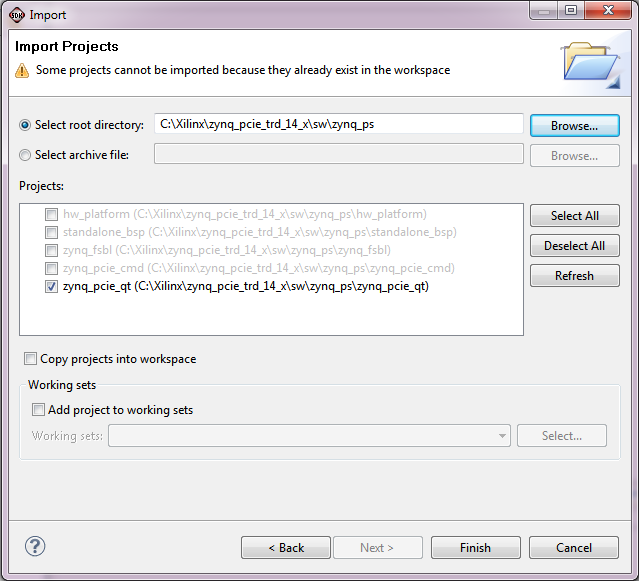
To import the Qt GUI Based SDK project (zynq_pcie_qt) into the SDK workspace, select File > Import.
In the Import wizard, expand the General folder, select Existing Projects into Workspace, and click Next.
All projects are located at the top-level inside your SDK workspace. Click Browse and navigate to $ZYNQ_TRD_HOME/sw. Press OK.
Make sure the zynq_pcie_qt project is checked. The hw_platform, zynq_fsbl, and -- if you have completed Section 9.1 previously -- the zynq_pcie_cmd projects will be grayed out since they have been added to your workspace already. Press Finish.
For this project, please uncheck the Project > Build Automatically option from the menu bar, otherwise you will receive an error message on the automatic build (see next step).
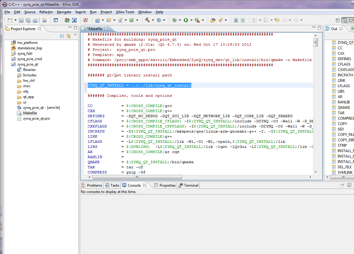
In the Project Explorer window, expand the zynq_pcie_qt project and double-click the Makefile to open it. Point the ZYNQ_QT_INSTALL variable in the Makefile to your Qt/Qwt libraries install area (refer to the Xilinx Zynq Qt Qwt Libraries - Build Instructions wiki for details).
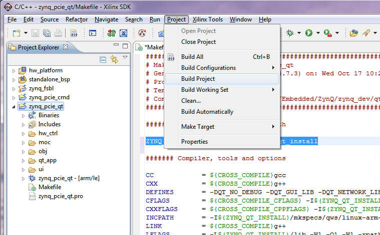
To manually build the project, right click zynq_pcie_qt in the Project Explorer and select Build Project; to clean the project, select Clean Project. The generated zynq_pcie_qt executable can be found at $ZYNQ_TRD_HOME/sw/zynq_ps/zynq_pcie_qt/zynq_pcie_qt.
10 Building the PCIe host SW application
The software application compilation procedure is provided here.
IMPORTANT: The traffic generator needs the C++ compiler which is not shipped with the Fedora 16 live
CD. Likewise, Java compilation tools are not shipped as part of the Fedora 16 live CD. Hence, GUI compilation will need additional installations. The source code is provided for an end user to build upon this design; for TRD testing recompilation of application or GUI is not recommended.
Steps for building the PCIe host software application
The source code (threads.cpp) for the Zynq-7000 PCIe TRD is available under the directory:
zynq_pcie_trd_14_x/sw/host/gui/jnilib/src
User can add debug messages or enable log verbose to aid in debug.
IMPORTANT: Changes in data structure will also lead to changes in the GUI compilation, which is not recommended.
To compile the traffic generator application:
1. Open a terminal window.
2. Navigate to the zynq_pcie_trd_14_x/sw/host/gui/jnilib/src directory and execute ./genlib.sh
Shared object (.so) files are generated in this same directory.
3. Copy all .so files to zynq_pcie_trd_14_x/sw/host/gui/jnilib directory.
TIP: Enable verbose messages by adding the -DDEBUG_VERBOSE flag to genlib.sh.
11 Running Demo Applications
This section explains through step by step instructions how to bring up the ZC706 board for video demonstration part of the TRD and running different video demonstrations out of the box.
The ZC706 Evaluation Kit comes with an SD-MMC card pre-loaded with binaries that enable the user to run the video demonstration and software applications. It also includes the binaries necessary to configure and boot the Zynq-7000 AP SoC based ZC706 board.
Note: If the evaluation kit design files were downloaded online, copy the entire folder ZYNQ_TRD_HOME/prog_qspi from the package onto the primary partition of the SD-MMC card (which is formatted as FAT32) using a SD-MMC card reader for loading the QSPI device with boot image and Linux kernel image. Once QSPI programming is over, load ZYNQ_TRD_HOME/sd_image content onto the primary partition of the SD-MMC card (which is formatted as FAT32) using a SD-MMC card reader for booting Linux and loading the QT application.
11.1 Hardware Setup Requirements
The ZC706 board setup to run & test the video demonstration applications require the following items:
Requirements for TRD Linux application demo setup
- The ZC706 evaluation board with the XC7Z045 FFG900-2 part
- Reference Design zip file containing BOOT.bin file, Linux kernel and Linux filesystem binary files, devicetree binary and application ELF. Host system driver and GUI files
- A control PC with ISE design Suite Logic Edition Tools v14.2
- A control PC with teraTerm pro (or similar) terminal program
- A control PC with USB-UART driver from silicon labs installed
- Mini USB cable
- USB mouse (not included with the kit)
- Class 4 equivalent SD card
- Monitor supporting 1080p
- HDMI cable
- 4-pin to 6-pin PCIe adapter cable
- Fedora 16 LiveCD
- PC with PCIe v2.0 slot. Recommended PCI Express Gen2 PC system motherboards are ASUS P5E (Intel X38), ASUS Rampage II Gene (Intel X58) and Intel DX58SO (Intel X58). Note the Intel X58 chipsets tend to show higher performance. This PC could also have Fedora Core 16 Linux OS installed on it.
Please note that two PCs are required for running this TRD. A control PC which is connected to the zc706 board via mini-USB running teraTerm and a host PC running Fedora Core 16 Linux connected to zc706 via PCIe slot on the motherboard
Note: The example mentioned in this package has been tested with Ivy Bridge and Sandy Bridge PCIe Host machine and a Dell model #P2412H display monitor. However, the example should work well with any HDMI-compatible output device.
11.2 Board Setup
For running the Host GUI and QT-based application on Zynq PS, please refer to Zynq-7000 SoC ZC706 Evaluation Kit UG961.
11.3 Running the Host GUI and Qt-based GUI Application on Zynq PS
For running the Host GUI and QT-based application on Zynq PS, please refer to Zynq-7000 SoC ZC706 Evaluation Kit UG961.
12 References
- Documentation for Zynq-7000 AP SoC
- Documentation for ZC706 Evaluation Kit
- Main Xilinx wik
© Copyright 2019 - 2022 Xilinx Inc. Privacy Policy