Zynq-7000 AP SoC Spectrum Analyzer part 6 - AMS - XADC Signal Acquisition and DMA to L2 Cache & Complete Design Tech Tip 2014.3
Zynq-7000 AP SoC Spectrum Analyzer part 6 - AMS - XADC Signal Acquisition and DMA to L2 Cache & Complete Design Tech Tip 2014.3
Table of Contents
Document History
| Date |
Version |
Author |
Description of Revisions |
|
| 23 October 2014 |
1.0 |
Faster Technology |
Initial posting - updated to 2014.3 |
|
| Date |
Author |
Comment |
||
|---|---|---|---|---|
| More Revisions |
||||
Description/Summary
In Tech Tip "Zynq-7000 AP SoC Spectrum Analyzer part 5 - Accelerating Software - Accelerating an FFT with ACP Coprocessor Tech Tip 2014.3" the FFT application developed in "Zynq-7000 AP SoC Spectrum Analyzer part 4 - Building and Running an FFT Tech Tip 2014.3" was enhanced by the addition of a hardware FFT implemented in the PL fabric of the Zynq-7000 AP SoC. This enabled us to compare execution times for the ARM processor, NEON SIMD engine and a pure hardware block, all computing the same FFT. The FFT application operates from data in an input table. Previously that data table was loaded with software generated data. In this Tech Tip, hardware will be added to the application in the PL to capture data from the on-chip Analog to Digital converter, the XADC block, connected to an AMS 101 or other appropriate analog input board.
This Tech Tip will illustrate the use of multiple DMA blocks and how the AXI interconnect can be used to funnel multiple processes into the ACP port of the PS. DMA operations are used for both moving the converted analog data into the PS and for filling and draining the hardware FFT block when that block is in use. This complication of the information flow is readily handled by the interconnect blocks in the PL design in coordination with the ACP port on the PS. Interrupts are used for signaling between the hardware blocks and the PS to reduce software overhead and demonstrate the ease with which interrupts can be used in a user application. In addition, this Tech Tip will demonstrate use of the IP Integrator (IPI) capability in Vivado 2014.3 for creation of the overall hardware system being utilized and coupling that to SDK for the software development and debug.
Implementation
| Implementation Details |
|
| Design Type |
PS & PL |
| SW Type |
Linux |
| CPUs |
1 CPU - standard ZC702 frequency |
| PS Features |
ARM Processor and NEON SIMD engine; OCM, DDR and other peripherals in standard PetaLinux OS environment |
| PL Cores |
Hardware FFT, XADC block AXI interconnect, AXI DMA |
| Boards/Tools |
ZC702 |
| Xilinx Tools Version |
Vivado / SDK 2014.3 and PetaLinux SDK 2014.2 |
| Other Details |
Standard ZC702 setup for console terminal and Ethernet required, 1920 X 1080P HDMI display, XA2 adapter card |
| Files Provided |
|
| **xadc_test.zip** |
Software application source code files to interface to XADC hardware in PL |
| **XADC2014DT3.zip** |
Vivado 2014.3 source files required to build XADC hardware interface in PL |
| **HWfft_workspace2014dt3.zip** |
Optional starting point workspace for software build process |
| **XADC_BOOT.zip** |
Optional BOOT.BIN file with XADC hardware in place |
Block Diagram

This Tech Tip relies on information used in the AMS Targeted Reference Design and builds upon some of the software supplied with that design. An implementation block diagram within Vivado will show the overall structure in a later section of this Tech Tip. The XADC block is initialized for the selected sample rate and the channel corresponding to the AMS 101 card installed on the ZC702. A DMA engine and AXI Stream to Memory map block is interfaced to the XADC to move the sample data. An AXI Interconnect block provides the interface to the ACP port on the PS, providing arbitration and multiplexing between the XADC data and the data flowing to and from the hardware FFT block. Inside the PS, data from the XADC transfer is stored in the FFT input buffer until a buffer full has been accumulated. At that point, the FFT is invoked, either in software or the hardware FFT block, to process the sampled data.
Step by Step Instructions
This Tech Tip proceeds in two major operations; building the Hardware FFT and then building the software that controls and uses the Hardware FFT in conjunction with the software in the PS. Vivado is used to build the hardware in the PL while PetaLinux SDK and Vivado SDK are used to build the software application that manages the hardware blocks and software computation of the FFT when requested.
Building the Hardware
Vivado 2014.3 will be used to create the hardware FFT and XADC interface used in this Tech Tip. The hardware design elements for this Tech Tip are derived from the sources supplied with the ZC702 base Targeted Reference Design (TRD) for Vivado 2014.2. This enables us to use the IP Integrator capability in Vivado 2014.3 to build the hardware required for the FFT block and the XADC control and data movement hardware. Additional IP blocks are supplied to supplement the base TRD with functions required for the XADC capability. This set of sources is combined in the XADC2014dt3.zip file associated with this Tech Tip.
If you have not yet downloaded XADC2014dt3.zip, do so now. It is best to save this at the root of a hard drive to avoid problems with long path names. In our instance we downloaded and unzipped XADC.zip to G:\XADC - the default if XADC.zip is saved to the root of the drive.
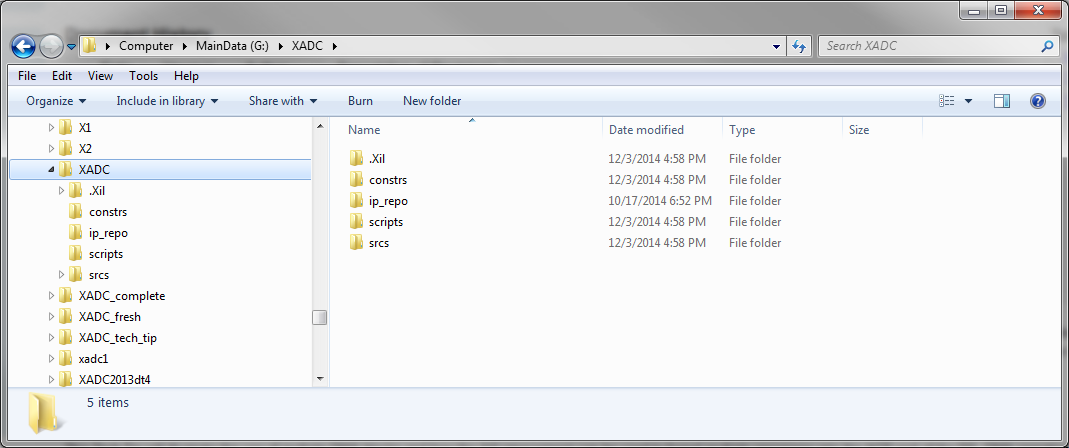
The base directory where the HWfft.zip files are saved is referred to as $ZYNQ_XADC_HOME. In our case then $ZYNQ_XADC_HOME is G:\XADC. If you have a different base directory, note that it will be used where $ZYNQ_XADC_HOME is referenced.
Supplied with this Tech Tip is a tcl script file that will simplify the process of building the FFT and XADC support hardware in Vivado. This file is:
project.tcl
The script file is in the /scripts sub directory where XADC was unzipped. In our case this is G:\XADC\scripts or
$ZYNQ_XADC_HOME/scripts
We now run Vivado to build the hardware system.
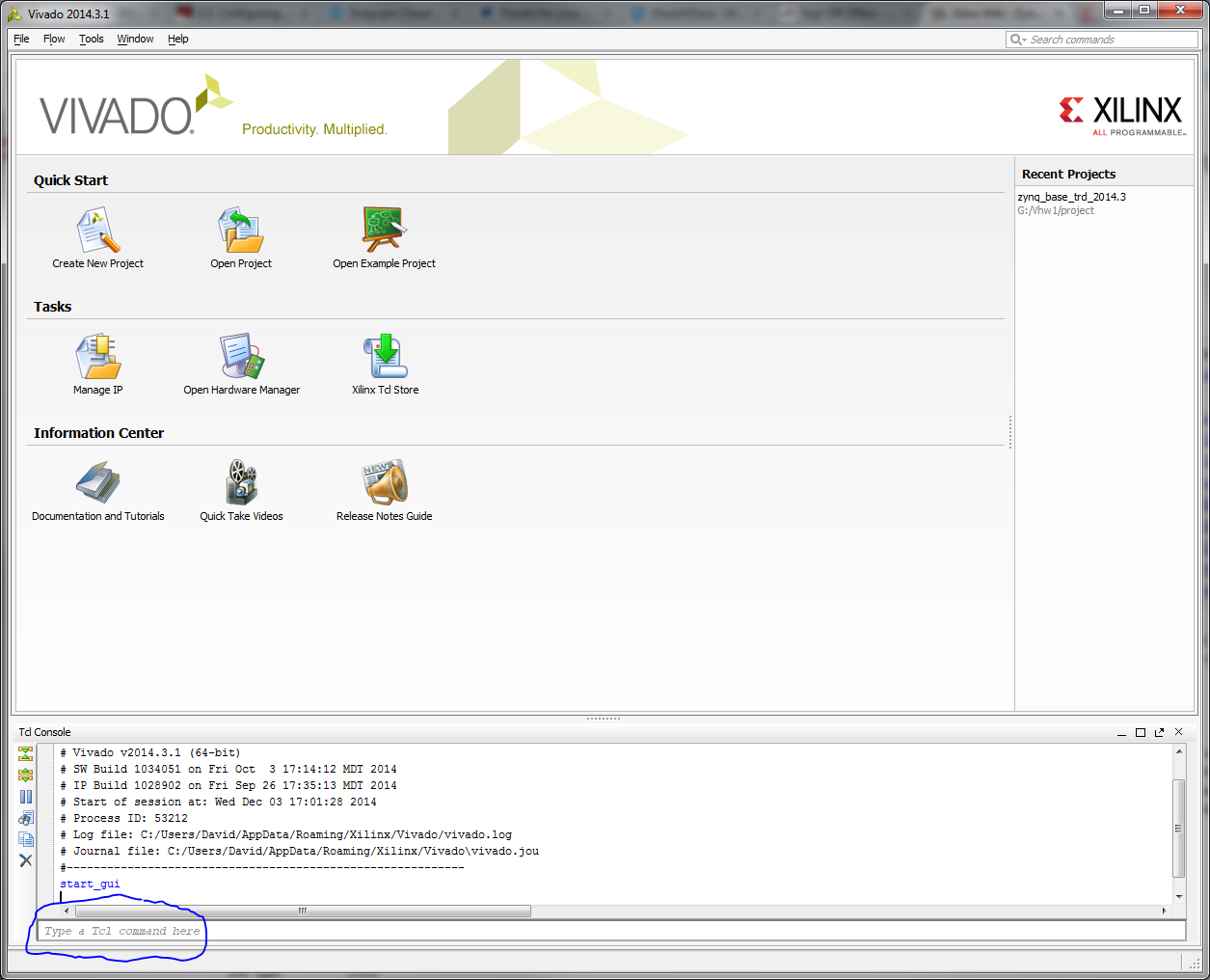
On Windows, select Start > All Programs > Xilinx Design Tools > Vivado 2014.3 > Vivado 2014.3
Vivado will start and show the welcome screen
CAUTION:
Before starting the process of building the hardware, verify that you have installed valid hardware licenses for the IP cores used in the ZC702 Base TRD design. These include the Chroma-Resampler, Video Timing Controller, etc. (See the Base TRD user guide for more information.) If a hardware implementation license is not in place when bitstream generation starts, the whole project will need to be deleted and started from the beginning.
In the tcl console input line, run the following commands
cd $ZYNQ_XADC_HOME
source . /scripts/project.tcl
The project.tcl should build the complete base TRD hardware system with the PS and various video processing hardware blocks used by the TRD software. In addition, it will add the FFT hardware block from the Tech TIp "Zynq Adding Hardware FFT Tech TIp" and the XADC block with additional hardware DMA support.
If you encounter any licensing issues or other implementation errors in running the project.tcl script, these must be resolved before running continuing. Otherwise the hardware will not build properly.
With this tcl script complete, the hardware FFT and XADC have been added to the system and connected to the PS as shown below
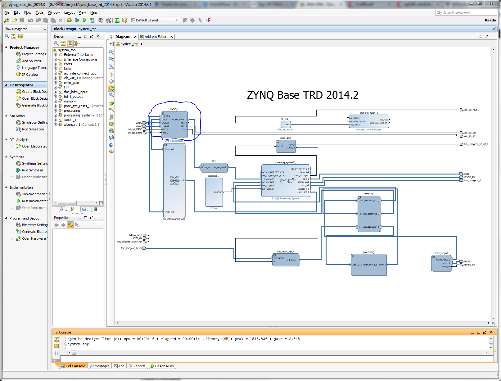
IP Integrator has both placed the functional blocks but also connected them with their corresponding signal bundles to the other blocks in the design. This greatly simplifies the process of generating a complex design and assuring that the components are connected properly. Any block of logic created from scratch or configured within Vivado can be saved as a reusable IP core for later use. See the Vivado IP Integrator documentation for details on how this is done.
In the block diagram pane, we can zoom into the XADC hardware to see what it contains. Move the cursor to hover over the upper left corner of the XADC block. When it changes to double chevrons, click to expand the hierarchy of the XADC IP core.
Using the zoom controls, either the magnifying glass with the + or selecting and dragging a zoom window in the diagram pane, zoom in to better see the contents of the XADC block. You can also maximize the diagram pane (click the maximize icon in the upper right corner) if desired.

The XADC block is a standard IP core that is configured through the Core Generator. In this instance it is configured to be controlled from the SPI interface that is exposed in the PS. This will enable us to use software to select the various possible inputs, set the sample rate, etc. When the software is built later in this Tech Tip, setup code from a reference design for the XADC block will be reused. This is facilitated by the use of the same physical and logical connections from the PS to the XADC core.
The axi_dma block previously seen in the hardware FFT implementation is used to move the data from the XADC into the FFT core. The AXI interconnect block is also used to move the data to the ACP port of the PS. The AXI interconnect handles any multiplexing and arbitration between the two AXI streams of data; from XADC and from the FFT processing block. In addition it handles the translation from streaming data, used by the FFT block to memory mapped data required to interface to memory in the PS through the ACP port.
The xlconcat block is used to vectorize the various interrupt sources in the design. For proper operation, interrupts from the PL to the PS must be enabled. To verify this, we examine the configuration of the ZYNQ7 Processing System block.
Double click on the Zynq block to enter it's configuration screens.
From the items in the left column, select "Interrupts" and click on it.
Expand the Fabric Interrupts item and the PL-PS Interrupt Ports line
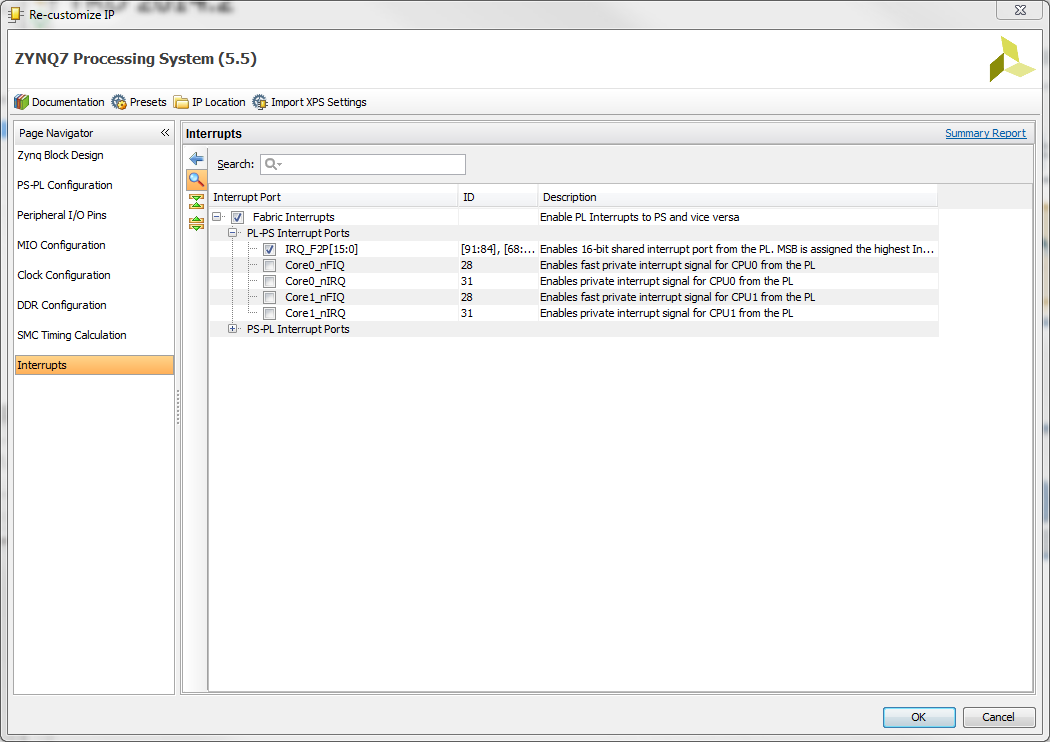
Note the range of interrupt numbers that are assigned to the IRQ-F2P inputs. As can be clearly seen, they are assigned to the higher order bits first; the first is 91, then 90, etc. These are the ARM A9 hardware interrupt numbers and are numbered differently in Linux. This will be noted later in discussing the device tree used by the kernal to manage the interrupts.
Also, the interrupt numbers are not contiguous, but that is not of concern for this application.
By expanding the PS-PL Interrupt Ports line, you can see that none of the possible interrupts from the PS into the Fabric are enabled; they are not used in this application.
With the interrupts enabled, we need to verify that they are connected properly in the hardware.
While the interrupts in the hardware are scaler items, the Interrupt handler in the PS expects a vector of interrupts. The Concat block will be used to concatenate all of the interrupt sources into a vector to be supplied to the IRQ_F2P port.
Exit from the Zynq Processing System configuration screen by hitting the Cancel button.
Double click on the Concat block (xlconcat_1) to enter its configuration screen.

In addition to interrupts already used in the TRD, we have added signals to monitor the read and write channels of the DMA used in the FFT block and the XADC block.
No changes to the Concat block are needed at this time so it can be exited by clicking the Cancel button.
While the build script has connected the interrupt sources to the Concat block, they may not be shown in the Block Design view within Vivado.
If the Block Design is not shown, click Open Block Design under IP Integrator in the Flow Navigator at the left side of the Vivado window.
With the Block Diagram shown, click on the icon at the top left corner of the Block Design Window adjacent to Block Design Options.
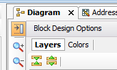
The items to be displayed will be listed. If display of interrupts is currently enabled (a check mark next to them) and they are not shown, simply disable and re-enable them.
We can now see the various interrupt sources connected to the Concat block

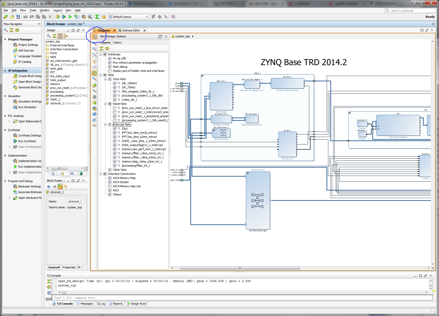
We will also need to know the location of the control registers used to manage the DMA block associated with the XADC. These are set properly by the build script so this step is just to illustrate how to check the addresses.
Click on the Address Editor tab at the top of the block design display window.
The address map of the hardware in the system will be shown. Note the address range for the AXI LITE interface for the XADC_1/axi_dma_1.
Return to the block design diagram by clicking on the Diagram tab on the block design display window.
To complete the hardware design, synthesis and implementation must be run. This can be done by initiating each step individually or if "Generate Bitstream" is selected, the Synthesis and Implementation steps will be run automatically.
In the flow Navigator panel, click Generate Bitstream (in the Program and Debug group at the bottom of the panel)
Synthesis, implementation and bitstream generation may take as long as two hours for this design. There will be some warnings, but these are not critical to the proper operation of the hardware. If there are any Launch Critical Warnings, simply click OK to accept them and allow Synthesis to continue.

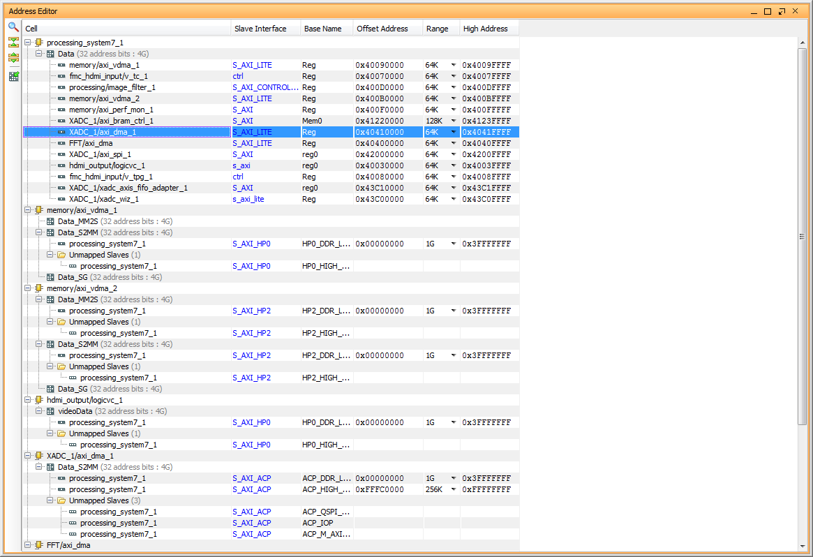
When Vivado completes processing the design, verify that there are no errors; warnings are expected with most relating to optimizations that are being done and have no impact on operation of the hardware. In the "Bitstream Generation Completed" accept the "Open Implemented Design option and click OK.
Vivado will then display the chip view of the implemented design
The next step is to export this hardware design in a form that SDK can use to build the files needed to properly configure the ZC702 to run the hardware FFT.
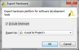
From the File menu select
File > Export > Export Hardware...

In the dialogue box that appears, leave the defaults selected and click OK. The option to Include bitstream should be visible and checked. This is convenient as it enables Vivado to put all of the information required in a single file.
Vivado creates a hardware description file in a directory branch off of the "project" area as shown below. The file in this branch will be used in the next step so remember where it is. (You may be prompted to save the project before the hardware is exported.)

At this point, we are done with Vivado and it can be closed. Save the project for future reference if prompted.
Building the Software
With the hardware for the FFT and the XADC block in the PL fabric complete and included in the base TRD hardware, we need to build the software to control the XADC and move data through the interconnect to the ACP port. Data received at the ACP port from the XADC operation will be placed in the FFT input table in the PS memory. When data receipt is complete, the DMA signals the PS of this action. In addition we will include the software developed in an earlier Tech Tip in this series to move data into and out of the FFT block. Recall from the block diagram that the data movement in the PL is controlled by DMA blocks. The software for operating the hardware FFT is simply the driver to start the DMA and to service the interrupts that are generated by the DMA block when it is complete. For the XADC block, software is used to set up the XADC through the control interface and to set up the DMA that moves the data into the ACP port. For the purposes of this Tech Tip, simple polling is used to monitor progress of the DMA associated with the XADC operation.
Building the software will be done in two separate steps; building a new boot file that includes the hardware for the XADC block and then separately building the application that controls the overall XADC operation and display of the results.
Building the BOOT.BIN file:
For this Tech Tip, interrupts are not being used for the interface to the XADC block. Therefore, the only boot file that needs to be built is the BOOT.BIN as it contains the bitstream which has the new hardware in the PL. In the previous Tech Tip "Zynq-7000 AP SoC Spectrum Analyzer part 6 - Accelerating Software - Accelerating an FFT with ACP Coprocessor Tech Tip 2014.3" the PetaLinux SDK was used to build both the BOOT.BIN and image.ub files. For this Tech Tip, we can use Vivado SDK because we are not building the image.ub file. Since we are only changing the bitstream portion of the BOOT.BIN, we will use a first stage boot loader (fsbl) and u-boot.elf files used by the PetaLinux system for the same operation.
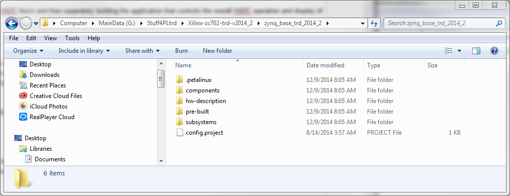
The base TRD for the ZC702 that utilizes PetaLinux is described in the technical article Zynq Base TRD 2014.2 Follow the instructions found there to download the software from the Xilinx web site. Unzip the set of files to a convenient place on your computer. In our case, we put them in our "Projects" folder:
G:\Projects\rdf0286-zc702-zvik-base-trd-2014-2
If we look inside this folder, we can see a variety of files but a fsbl and u-boot.elf are not readily apparent. However, there is a large file with the extension of .bsp that is in the petalinux folder. Normally this is used to set up a project within the PetaLinux development environment. For our use, we are going to extract the needed boot files from this .bsp file.
G:\Projects\rdf0286-zc702-zvik-base-trd-2014-2\software\petalinux\bsp\Xilinx-zc702-trd-v2014_2.bsp
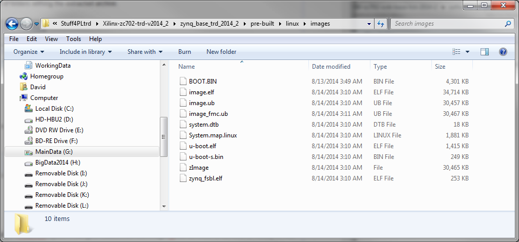
While we could extract the contents at the current location, to be sure we do not disturb the integrity of the TRD, we simply copy the .bsp file to another location. Once that is done, change the extension to .tar (this file is really a compressed Linux compatible file). Then we can use a standard tool to "un-compress" the file, resulting in the following set of folders withing the extracted archive.
If we then drill into the pre-built folder to linux and then images, we can find the following set of files
From within SDK, we will simply use the now readily visible zynq_fsbl.elf and u-boot.elf files along with the new bitstream to build the required new BOOT.BIN file.
At the conclusion of the Tech Tip "Zynq-7000 AP SoC Spectrum Analyzer part 5 - Accelerating Software - Accelerating an FFT with ACP Coprocessor Tech Tip 2014.3" the workspace contains the library of signal processing functions built in the Tech Tip "Zynq-7000 AP SoC Spectrum Analyzer part 2 - Accelerating Software - Building ARM NEON Library Tech Tip 2014.3"and tested in the Tech Tip "Zynq-7000 AP SoC Spectrum Analyzer part 2 - Accelerating Software - Running ARM Library Tests Tech Tip 2014.3". It also has the tested application code for the FFT application including the hardware FFT. This Tech Tip is built upon that existing workspace. If you have that workspace in place,skip forward in these instruction to where the workspace is in place (Old Workspace in Place).
If the workspace is not available, or if there is an question if it was completed properly (or you simply want to skip those earlier steps), the referenced file HWfft_workspace2014dt3.zip can be used to create a known working starting point for the software portion of this Tech Tip.
Download the zip file from the HWfft_workspace2014dt3.zip link.
Create an empty directory where you will be implementing this Tech Tip. To be consistent with the balance of these step by step instructions, the directory could be:
G:\Projects\ZC702_Ne10
However, these steps to import a known workspace will work with any new folder of the user's choosing.
CAUTION:
Many users have unusual problems with SDK when using different directory structures or names. If you encounter any odd behaviors with SDK, it is advised to use the suggested directory structure and names.
Start SDK
Start -> All Programs -> Xilinx Design Tools -> Vivado 2014.3 -> Xilinx SDK 2014.3
In the Workspace Launcher, browse to and select the previously created empty folder. In our case, that is G:\Projects\ZC702_Ne10
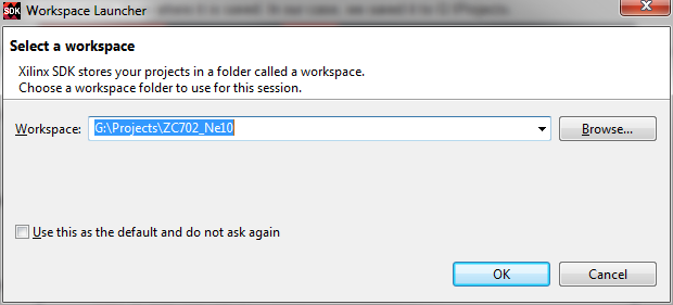
Click OK to continue
If you are presented with a Welcome tab, close it by clicking on the x on the tab.
SDK will start with a blank Project Explorer pane
Select File -> Import
The Import dialogue box will appear. Expand the General line and select Existing Projects into Workspace
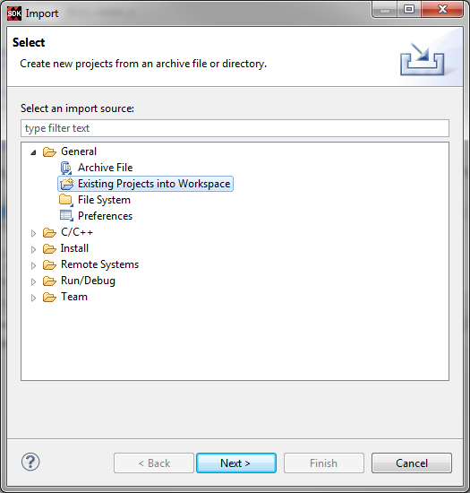
Click Next
Click the Select archive file button. Then click Browse to navigate to the saved workspace file that you want to import and click Open. In our case this is HWfft_workspace2014dt3.zip.
Click Finish
SDK will build the workspace automatically. If it does not, simply select Project -> Build All
Because SDK is now running and the workspace is in place, you can skip the following instructions on starting SDK and go directly to after SDK is running and the workspace is in place (Starting Projects Ready).
Old Workspace in Place
The first step in building our new BOOT.bin is to bring the new hardware information from Vivado into SDK. We start with the workspace that resulted from the completion of the "Zynq-7000 AP SoC Spectrum Analyzer part 5 - Accelerating Software - Accelerating an FFT with ACP Coprocessor Tech Tip 2014.3".
Start SDK
On Windows, select Start -> All Programs -> Xilinx Design Tools -> Vivado 2014.3 -> Xilinx SDK 2014.3
When the Workspace Launcher appears, be sure that it is pointed to the workspace used for the "Zynq-7000 AP SoC Spectrum Analyzer part 5 - Accelerating Software - Accelerating an FFT with ACP Coprocessor Tech Tip 2014.3".
Click OK
Starting Projects Ready
SDK should have the files and projects in place as we last saw them. If it has changed, use the known workspace from the steps above or repeat the various steps to be sure this is a tested working set of files and projects before proceeding.
The new hardware from Vivado will impact the standalone_bsp and the hardware platform (ZC702fft in our case) which in turn are key in building any hardware dependent applications, such as the XADC test software. These changes also would impact creating of new files for building a new BOOT.bin but we will not need to do that here as we will extract them from the PetaLinux build package as described earlier.
Select the hardware platform - in this case we have called it ZC702ff - in the Project Explorer pane, right click on it and select "Change Hardware Platform Specification". When the pop up box appears, read the cautions and click Yes.

Click Browse and follow the path from the $ZYNC_XADC_HOME used earlier to \project\zynq_base_trd_2014.3.sdk
SDK will show system_top_wrapper.hdf as an available file.
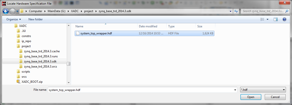
Select system_top_wrapper.hdf
Click Open and then OK in the "Change Hardware Platform Specification" dialog
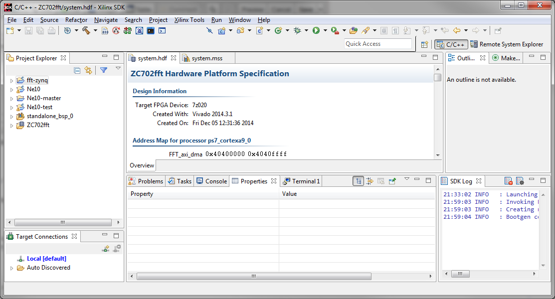
SDK will process the new Hardware Description File (.hdf) and update the current platform.
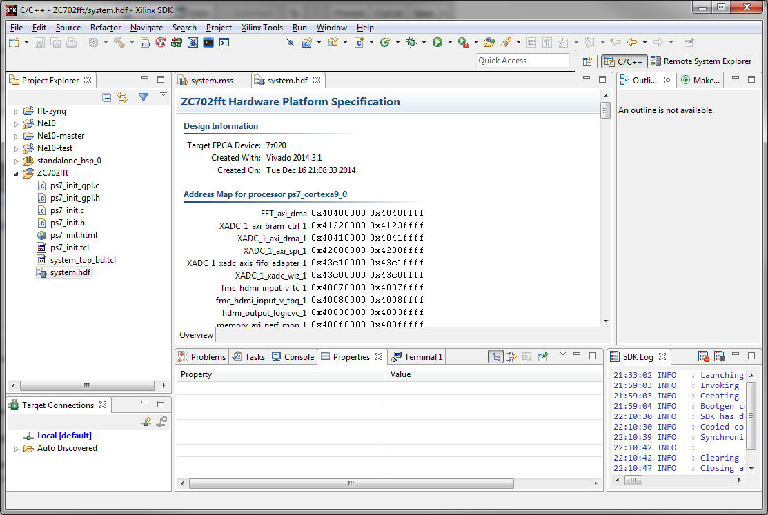
To verify this update, expand the ZC702fft line in the Project Explorer pane and double click on system.hdf. SDK will display the current information about the hardware system. Note the presence of several items relating to XADC, and note the address of the XADC_1_axi_dma_1 which we noted earlier in examining the hardware from within Vivado.
To complete the inclusion of the new hardware information we need to re-build the Board Support Package (bsp). In this case this is the project called standalone_bsp_0 (Note that it has a different leading icon to indicate it is a board support package.).
There are two approaches to updating the Board Support Package. One way is to delete the current bsp from the system (if you do this be sure to check the selection box to delete it from your computer), and build it from scratch as was shown in an earlier Tech Tip. The second approach used here is to force a regeneration from the hardware platform.
Select standalong_bsp_0 in the Project Explorer pane. Right click and select Re-generate BSP Sources. This will update the BSP with appropriate interfaces and drivers for the new hardware.
When that is finished, right click on standalong_bsp_0 again and select Clean Project. When that is finished, right click on it again and select Build Project.
The build process will create an error similar to the following:
xsysmon_g.c:53:3: error: 'XPAR_XADC_1_XADC_AXIS_FIFO_ADAPTER_1_IP_TYPE' undeclared here (not in a function)
XPAR_XADC_1_XADC_AXIS_FIFO_ADAPTER_1_IP_TYPE
At this time, the cause of this error is under investigation. However, it can be readily remedied.
In the Project Explorer pane, navigate into the standalone_bsp_0 project to the following:
standalone_bsp_0 -> ps7_cortexa9_0 -> libsrc -> sysmon_v7_0 -> src -> xsysmon_g.c
Double click on xsysmon_g.c to open it in an edit window in SDK
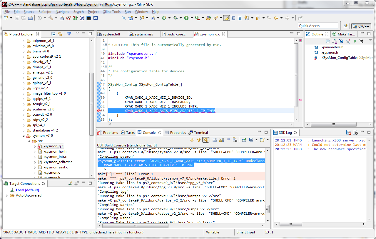
Change the highlighted line to be
XPAR_XADC_1_XADC_WIZ_1_IP_TYPE
Save the file by selecting File -> Save from the main menu.
Re-build the BSP by first cleaning it - right click on standalone_bsp_0 and select Clean Project. When that is finished, right click on it again and select Build Project. The build should proceed without errors.
NOTE:
If other changes are made to the hardware platform or to the bsp, Re-generate BSP Sources operation will overwrite this change with a new file so it will need to be manually changed again.
With the system updated with the new hardware information we will proceed to build the BOOT.BIN file that includes the new hardware. As noted, we will use files extracted from the PetaLinux build system archive.
From the main menu bar select
Xilinx Tools -> Create Zynq Boot Image
The dialogue box where the boot file is created will be shown.
The BIF file describes the contents of the file that is being built and any special options, etc. It enables a new boot file to be created automatically with the same settings and file names.
In this case there is no BIF file.
Click the Browse button adjacent to the description box for Output BIF file. Select a location to save the BIF file. In our case, we are saving the file in the same directory where we initiated the hardware build: G:\XADC

Note that this operation also sets the location where the BOOT.bin file will be saved.
Now we add the files which are used to build BOOT.bin. Three files are required to create BOOT.bin
- A first stage boot loader
- A valid bitstream
- A u-boot.elf executable that will load the operating system and any applications after the system is started.
CAUTION:
These files MUST be in the order stated above for proper boot operation!!
First Stage Boot Loader:
Recall earlier where the PetaLinux bsp file was copied to, renamed, and unzipped. We specifically called out the images folder. In our case this was:
G:\Stuff4PLtrd\Xilinx-zc702-trd-v2014_2\zynq_base_trd_2014_2\pre-built\linux\images
In the Create Zynq Boot Image dialogue (it should still be open) click on the Add button on the right side of the Boot image partitions box. In the Add Partition dialogue, click on browse and navigate to the location of the images folder and select
zynq_fsbl.elf
Then click Open. This will populate the Add Partition dialogue box.
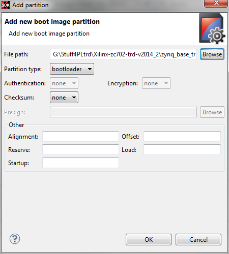
Click OK
Valid Bitstream
The bitstream default location is in the project folder where Vivado was started to build the XADC hardware.
With the Create Zynq Boot Image dialogue still open, again click the Add button on the right side of the Boot image partitions box. In the Add Partition dialogue, click on browse and navigate to the location of the bitsteam. It will be at $ZYNQ_XADC_HOME\project\zynq_base_trd_2014.3.runs\impl_1
Select the bitstream - the default file name is:
system_top_wrapper.bit
Click Open and when the Add Partition dialogue appears, click OK
u-boot.elf
Using the same steps as we did for the zynq_fsbl.elf file, we will add the u-boot.elf.
In the Create Zynq Boot Image dialogue (it should still be open) click on the Add button on the right side of the Boot image partitions box. In the Add Partition dialogue, click on browse and navigate to the location of the images folder and select
u-boot.elf
Click Open and when the Add Partition dialogue appears, click OK
We should now have the 3 files loaded and in the proper order as shown below.
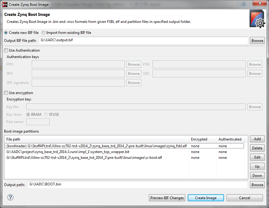
Click the Create Image button to create the BOOT.bin file.
The new BOOT.BIN file now includes the additional hardware for the XADC and FFT blocks. At this point we have not modified the PetaLinux system that gets loaded from the image.ub file so there is no need to modify it. The application built in the following section will simply be invoked as an application running on the PetaLinux after it has booted.
Building the Application:
With the fft hardware included in the new BOOT.BIN file we can now build the application which will interact with the hardware.
If you have not already done so, download the xadc_test.zip which is an archived project for SDK. We now use that archive to build the application which controls the XADC hardware added to our system.
Because we started with the workspace where we built the software for the " Zynq-7000 AP SoC Spectrum Analyzer part 5 - Accelerating Software - Accelerating an FFT with ACP Coprocessor Tech Tip 2014.3", we already have a fft-zynq project defined. We will now add a separate project that supports the XADC capability needed for this Tech Tip. The project has a top level set of files and two sub directories that will be imported as a complete project.
Start the File Import dialog in one of at least two ways; a) Right click on blank space in the Project Explorer window. From the pop up menu, select Import or b)From the top menu bar select File > Import
In the Import select dialogue box, expand the General category and select "Existing Projects into Workspace".
Click Next
Click the button next to Select archive file, then click Browse
Navigate to where you saved the archived project; in our case G:\Stuff4PLtrd
Select xadc_test.zip and click Open
The possible projects will be listed. If it is not already selected, click the box next to the xadc_test project in the list.

Click Finish to import the files
The new project will appear in the Project Explorer pane

Before building this imported project, we need to be sure the Paths and Symbols are set correctly.
Right click on the xadc_test project in the Project Explorer pane. From the pop up menu, select C/C++ Build Settings
Expand the C/C++ General category and then select Paths and Symbols.
Some paths may already be set from the process of creating this project. If the Include Directories pane has an item that begins with /zynq_fsbl ... this will need to be changed. Select that item and click the Delete button on the right side of the window. We now will set the correct path so SDK will use the updated hardware settings from the Vivado export process.
Click the drop down arrow for the Configurations line and select All Configurations (if desired, separate selections can be made for Debug versus Release builds but that is not recommended in this case).
Click the Add button on the right side of the dialogue box
In the Add directory path dialogue box, click both of the options then click the Workspace button and expand the standalone_bsp_0 folder and then expand the ps7_cortexa9_0 and select the include sub directory

Click OK
When the Add directory path dialogue appears, Click OK to save the include path.
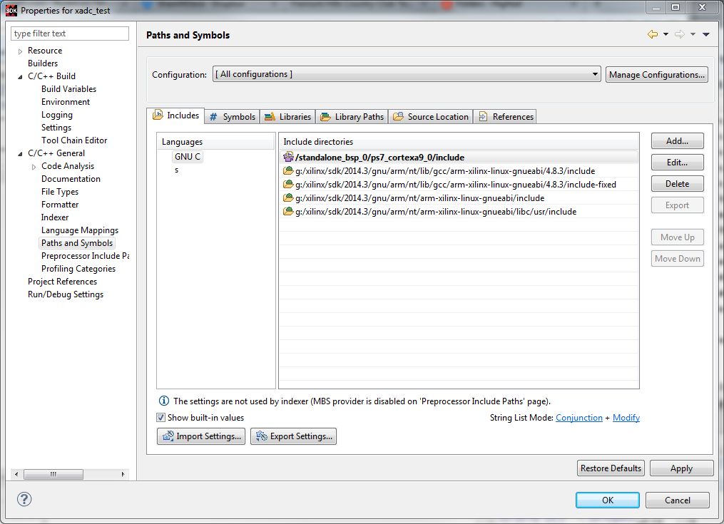
Click Apply
If the warning message appears regarding indexing, click Yes.
Click OK to finish adding the paths
We also need to verify that a standard library will be used in the linking process.
Right click on the xadc_test project in the Project Explorer pane. From the pop up menu, select C/C++ Build Settings
Expand the C/C++ Build category and then select Settings.
In the right pane, under ARM Linux gcc linker, click Libraries
The list of libraries should appear as below. Be sure that Release is selected in the Configuration: line
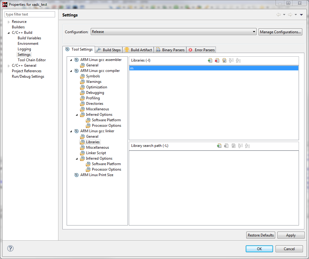
If the library m is NOT listed in the Libraries(-l) list box. we need to add it. To do this
Click the green plus icon at the top of the Libraries list box.
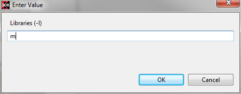
type m in the entry box and click OK
The standard library m will appear in the list as shown above.
Click Apply and then Click OK to set the Libraries properly.
One other minor change to the xadc_test source code is required for it to build properly in this environment.
Click on xadc_test in the Project Explorer pane. Navigate to xadc_test -> src -> xadc_core.c then double click on it to open it in an edit window in SDK.
The current version will appear as shown in the right half of the WinMerge screen below. Make the following changes so it appears like the left half of the screen below:
- remove the first line that begins with typedef
- Move lines 2 through 11 to just after old line number 28.
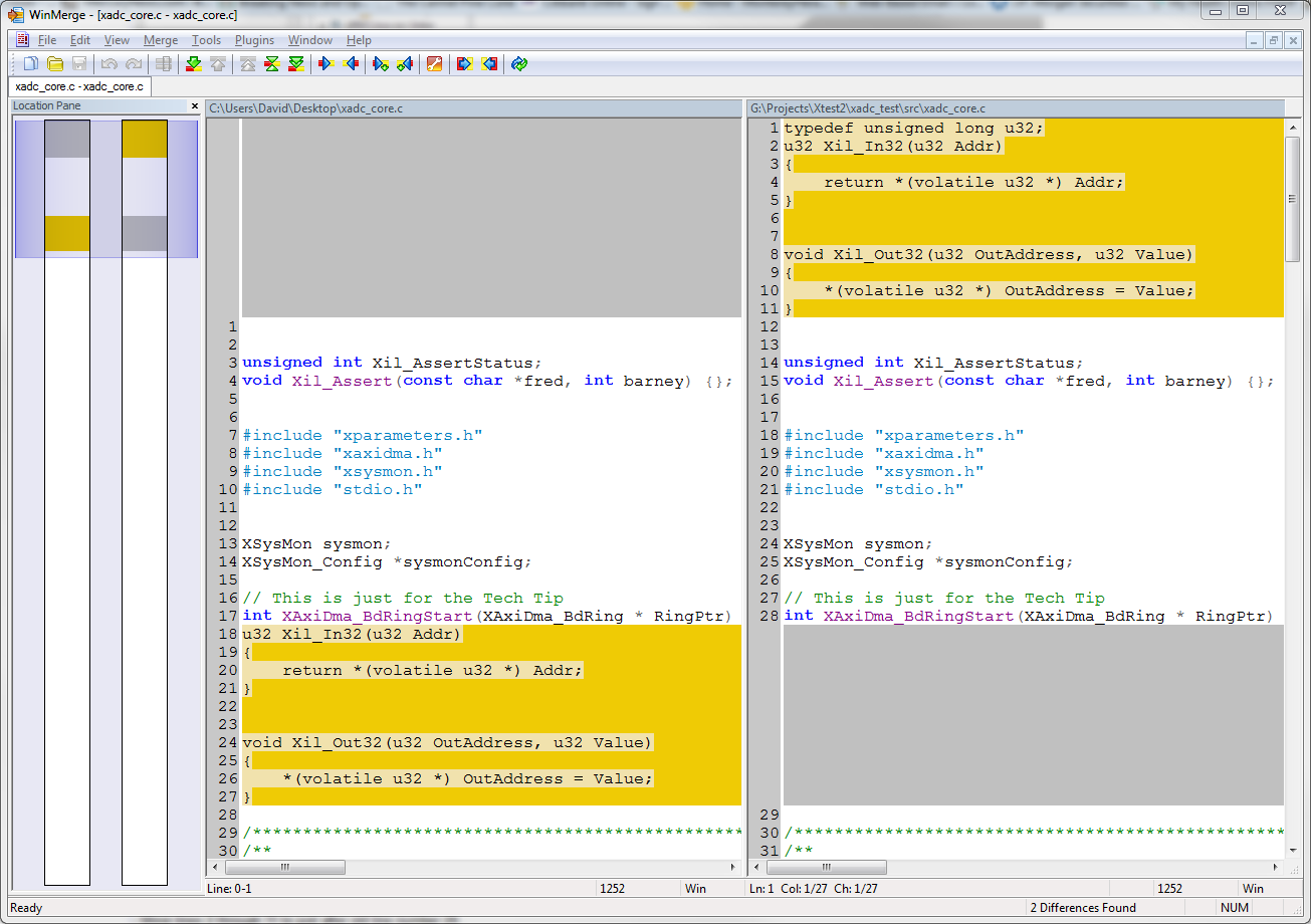
Save the application by selecting File -> Save from the main menu bar.
We can now build the application software.
To be sure we are using the Release build options (for best performance), Right Click on the xadc_test project in the Project Explorer pane, then select Build Configurations -> Set Active -> Release
Right click on xadc_test and select Clean Project from the pop up menu. When that completes, right click on xadc_test and select Build Project from the pop up menu. SDK will then build the new application software.
Testing the XADC hardware system
With the new BOOT.bin and xadc_test.elf application files completed, we can test them and verify that the XADC system is capturing data properly.
The BOOT.bin file replaces one already on the SD card used to boot the ZC702. With the power to the ZC702 OFF, remove the SD card and insert it in a SD card reader or media slot on your computer. The files on the card should be at least this set
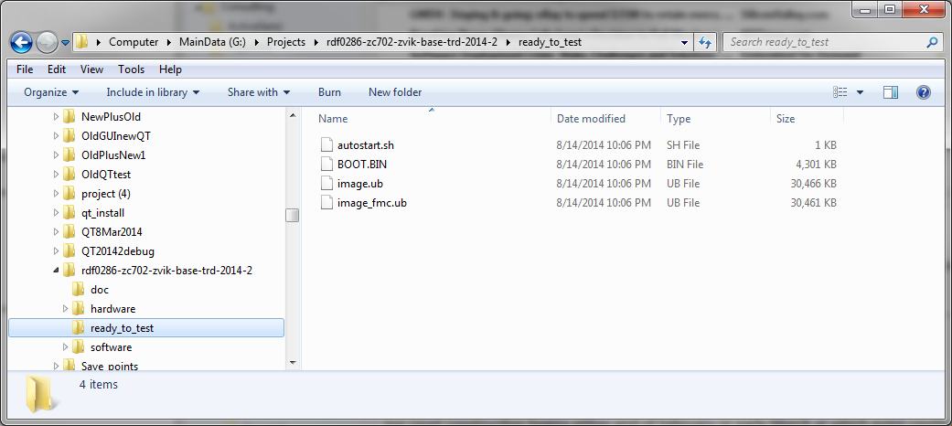
If the base set of files are different in any way, it is wise to delete the files on the SD card and copy a new set to it before proceeding. A new set of base TRD files can be found in the un-zipped TRD in the ready_to_test directory as shown above. Standard Windows copy / paste can be used to copy the files to the SD card.
Once the SD card files have been checked, delete the BOOT.bin file on the SD card (or rename it to something completely different).
Locate the BOOT.bin file we just created in SDK, In our case we saved it to the directory from which Vivado was used to build the XADC hardware
G:\XADC
Copy BOOT.bin and then paste it to the SD card.
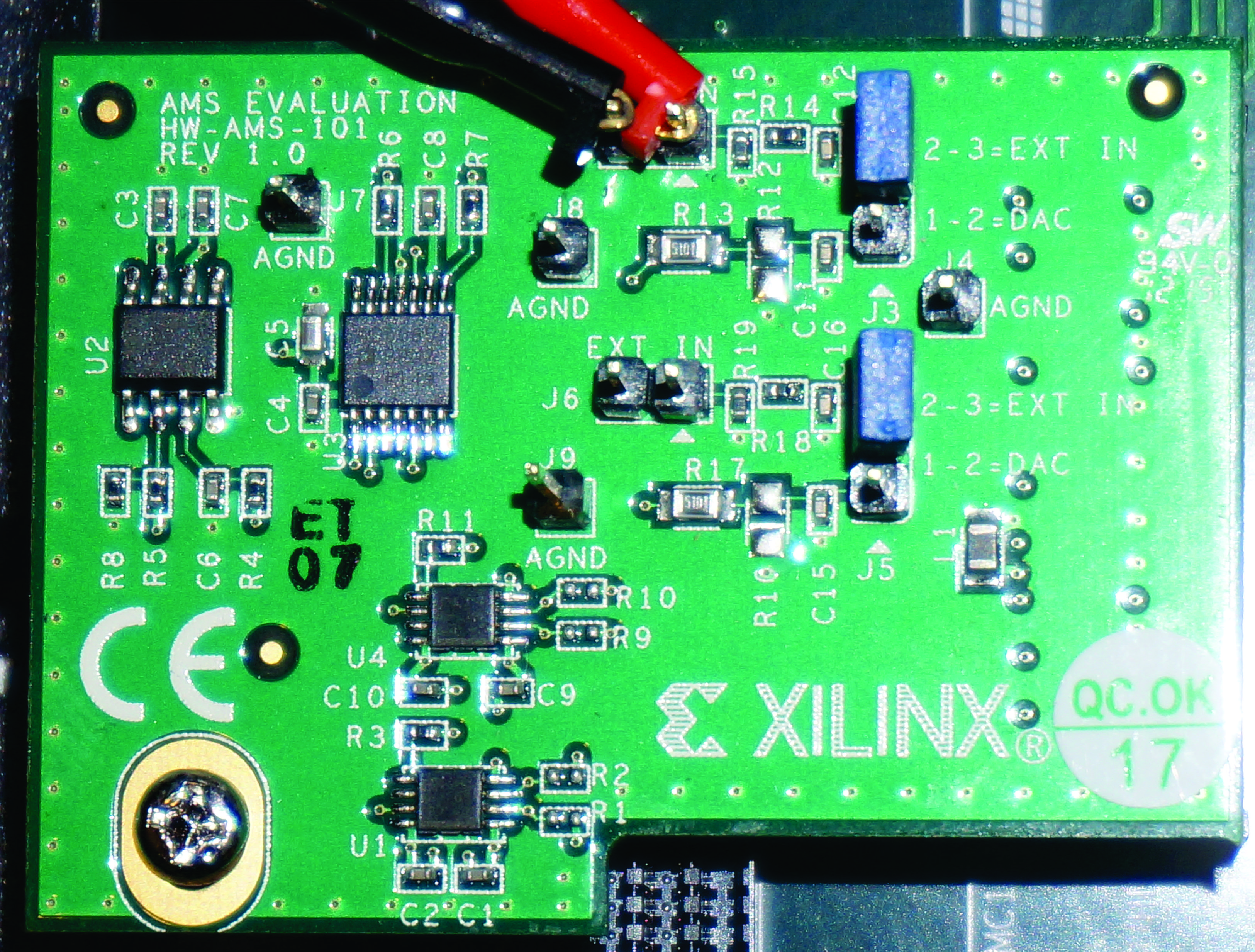
Mount the AMS 101 card on the ZC702 as described in the user guide for the card. We will be using an external input on one of the two channels so set the jumpers as follows:- J3 - connect pins 2 and 3 to select External Input- J5 - connect pins 2 and 3 to select External Input
To exercise the xadc_test application and the corresponding XADC hardware system, we need an input source for the AMS 101 card. The input to the AMS card MUST be in the range of 0.0 to 1.0 Volts. this can be accomplished with a signal generator where the offset is at 0.5 volts and the input signal is limited to 1.0 Volts peak to peak. Before connecting to the AMS card, use an oscilloscope to verify that the input is within the range of 0.0 to 1.0 Volts.
Remove the SD card from your computer, insert it into the ZC702 and power on the ZC702. The ZC702 should boot and run the standard TRD demonstration.
With the input signal levels verified, connect the signal source to the AMS card on J2 as shown below. For simplicity of viewing the sampled data, a square wave offers a readily recognizable sample pattern.
Once the ZC702 has booted and the Sobel Filter demonstration is running, exit from the demo to return to Linux. We can then use Remote System Explorer to run the application. As an alternate, we could copy the xadc_test.elf application file to the SD card when we changed BOOT.bin and run it from the command line on the ZC702.
For RSE operation, we use the same steps as used in the previous Tech Tips. They are summarized here for simplicity.
CAUTION!!
The default IP address of the ZC702 is different for PetaLinux than for the OSL Linux used in prior versions of this series of Tech Tips. The default IP address is now 192.168.0.10 so be sure your computer can reach that sub-net.
Connect your ZC702 to your computer or network with an Ethernet cable.
If you are unable to directly reach the .0 subnet from your computer, it is possible to change the IP address of the ZC702 after PetaLinux has booted. To make this change, do the following:
- Connect the console serial over USB port to your PC with the supplied mini-usb adapter and appropriate cable
- Start TeraTerm or similar terminal emulator
- Boot the ZC702 as described below
- Once PetaLinux has booted, log in using the username root and password root
- Use the ifconfig command to change the IP address using - "ifconfig eth0 192.168.1.65" where the IP address is one that you can reach from your PC - in this case we are using 192.168.1.65 for the balance of this Tech Tip.
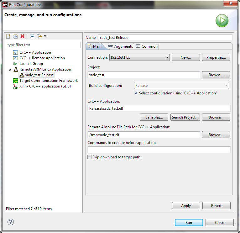
Right click on xadc_test and select Run As from the pop up menu, then select Remote ARM Linux Application. Because we have used SDK and RSE in the prior Tech Tips, all of the entries will be filled in and you can simply select Run. If prompted for the password, recall that it is root.
To verify operation of the XADC hardware system, we run xadc_test.elf in a command line mode. This enables us to run it once and display the data. Verify the setup of the run configuration and then select the Arguments tab.
Enter the following in the Arguments pane:
-g 64
This will force xadc_test to execute once and display the first 64 samples of input data.
Click the Main tab and verify that the setup is correct.
CAUTION:
If the -g option is not specified, the XADC will be set up for continuous sampling and will not stop to display the results as expected. If this is done, it may be necessary turn off the ZC702 and start the RSE process again.
Start the signal source and select a frequency (for this test we used ~6.5 KHz.) and an amplitude less than the maximum and select a square wave. The square wave is readily recognizable in the output data table.
Click Apply and then Click Run
RSE will launch the xadc_test application on the ZC702. The results will be displayed in the console pane. If xadc_test does not halt after one pass, try clicking the large red X at the top of the console window to cause it to halt.
For an alternate method to gather some sampled data, we can switch to a RSE perspective and run the application directly from SDK using Linux commands.
Depending on how the options are set for your SDK installation, you may have a Remote System Explorer icon in the upper right corner of the SDK window. Click on that to get a RSE perspective. Otherwise, from the main menu bar select Window > Open Perspective > Other.
In the selection box, click Remote System Explorer and click OK
In the left pane, right click on Ssh Terminals and select Launch Terminal
A terminal for the ZC702 will be opened

From this terminal pane (maximize it to see the largest output stream) enter the following commands:
cd /tmp
./xadc_test.elf -g 512
This will run the fft_backend application a single time and print the first 512 samples of input data. From this pane it is possible to copy the sample data and paste it into a spreadsheet for further analysis and display.
Conclusions
Using the same DMA techniques as in previous Tech Tips enables us to capture sample data from the XADC block and operate on it from Linux in the PS. While the output in this Tech Tip is simply a dump of the sampled data, it is clear that this data can be the input of other processes. Most notably, we can use this input data with the FFT application in the Tech Tip "Zynq Building an FFT Application Tech Tip" and "Zynq Adding Hardware FFT Tech Tip".
The Zynq-7000 AP SoC offers a powerful combination of general purpose processing in the PS and hardware processing in the PL. This coupled with the Analog to Digital conversion capability enables a wide variety of highly integrated applications.
The use of standard building blocks with IP Integrator in Vivado enables rapid addition of hardware to the existing Zynq-7000 AP SoC platform. By using the same physical and logical connectivity as other reference designs, we can rapidly build a new system with proper control and data management between the PS and PL within the device.
© Copyright 2019 - 2022 Xilinx Inc. Privacy Policy