 Introduction
This documents provides the details about the Pl35x smc and pl35x nand drivers located in drivers/memory/pl353-smc.c and drivers/mtd/nand/raw/pl35x-nand-controller.cLink for the source files: pl353-smc.c and pl35x-nand-controller.c
The SMC (PL353) supports two memory interfaces:
- Interface 0 type SRAM/NOR.
- Interface 1 type NAND.
For NOR, it is generic Linux CFI driver.
HW/IP Features
Controller Features
- ONFI 1.0 compatible
- supports up to 1GB device
- 8/16-bit IO width with a single chip select
- 16-word read/write FIFOs
- 8-word command FIFO
- Programmable IO Cycle timing
- 1-bit ECC hardware with sw assist
- Asynchronous memory operating mode
Driver Features
- Supports only the mandatory ONFI 1.0 commands. i.e Reset, Read status, Read ID, Read Parameter Page, Read Page, Program Page, Erase Block, Set/Get Features
- Supports BBT management
- Supports ondie ecc devices
- Support for hw ecc and sw ecc
- support for 8 and 16 bit flash devices
- Support for configuring the nand and nor timing parameters
Missing Features, Known issues, limitations
- HW ecc support for devices with 2K page size up and oobsize up to 64 bytes. Beyond that the driver will choose sw ecc mechanism.
Bad Block management
As part of the bbt management, driver reserves the last 4 blocks of the flash device for storing the bbt information. bbt management is similar to the standard Linux algorithm except the offset of storing the BBT signature and version; and also the locations reserved for storing the ecc information.Kernel Configuration options
SMC Driver
The following kernel configuration options should be enabled for compiling the pl353 smc driverDevice Drivers -> Memory Control Drivers -> ARM PL353 Static Memory Controller(SMC) driver
CONFIG_ARM = y
CONFIG_PL353_SMC = y

NAND Driver
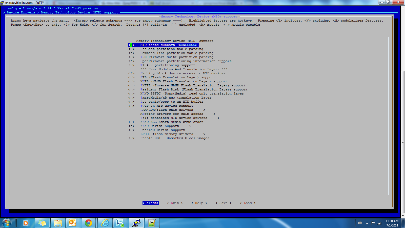
The following kernel configuration options should be enabled for compiling the pl353 smc nand driverDevice Drivers -> Memory Technology Device (MTD) support -> NAND - > Raw/Parallel NAND Device Support ->ARM PL353 NAND flash driver
CONFIG_MTD_NAND = y
CONFIG_ARM = y
CONFIG_PL353_SMC = y
CONFIG_MTD_NAND_PL35X = y

NOR Driver
Select the Device Drivers option and then, select Memory Technology Devices (MTD).Finally, choose the RAM/ROM/Flash chip drivers option.
Detect flash chips by common flash interface (CFI) by selecting one of the following:
- For the static build, choose the option <*> Detect flash chips by Common Flash Interface (CFI).
- For build as a module, choose the option <M> Detect flash chips by Common Flash Interface (CFI).
- For static build, choose the option <*> Support for AMD/Fujitsu flash chips.
- For build as a module, choose the option <M> Support for AMD/Fujitsu flash chips.
- For static build, choose the option <*> Support for Intel/Sharp flash chips.
- For build as a module, choose the option <M> Support for Intel/Sharp flash chips.
- For static build, <*> Flash device in physical memory map based on OF description
- For build as a module, <M> Flash device in physical memory map based on OF description


Device Tree
For more details on nand devicetree details, please refer pl353-smc.yamlThe timing parameters t0, t1, t2, t3, t4, t5, t6 denotes
nand-cycle-t0 : Read cycle time(t_rc).
nand-cycle-t1 : Write cycle time(t_wc).
nand-cycle-t2 : re_n assertion delay(t_rea).
nand-cycle-t3 : we_n de-assertion delay(t_wp).
nand-cycle-t4 : Status read time(t_clr)
nand-cycle-t5 : ID read time(t_ar)
nand-cycle-t6 : busy to re_n(t_rr)
NAND Node:
--------------
		memory-controller@e000e000 {
        	compatible = "arm,pl353-smc-r2p1", "arm,primecell";
             reg = <0xe000e000 0x1000>;
             status = "okay";
              clock-names = "memclk", "apb_pclk";
              clocks = <0x1 0xb 0x1 0x2c>;
              ranges = <0x0 0x0 0xe1000000 0x1000000 0x1 0x0 0xe2000000 0x2000000 0x2 0x0 0xe4000000 0x2000000>;
              #address-cells = <0x2>;
              #size-cells = <0x1>;
              interrupt-parent = <0x4>;
              interrupts = <0x0 0x12 0x4>;
              phandle = <0x26>;

              nand-controller@0,0 {
					compatible = "arm,pl353-nand-r2p1";
                    reg = <0x0 0x0 0x1000000>;
                    status = "okay";
                    #address-cells = <0x1>;
                    #size-cells = <0x0>;
                    phandle = <0x27>;

                    nand@0 {
							reg = <0x0>;
                            #address-cells = <0x1>;
                            #size-cells = <0x1>;
                            nand-ecc-mode = "hw";
                            nand-on-flash-bbt;

                            partition@0 {
                            	label = "nand-fsbl-uboot";
                                reg = <0x0 0x10000000>;
                            };
                     };
              };
	 };

NOR node:
---------
		smcc: memory-controller@e000e000 {
			#address-cells = <1>;
			#size-cells = <1>;
			status = "disabled";
			clock-names = "memclk", "apb_pclk";
			clocks = <&clkc 11>, <&clkc 44>;
			compatible = "arm,pl353-smc-r2p1", "arm,primecell";
			interrupt-parent = <&intc>;
			interrupts = <0 18 4>;
			ranges ;
			reg = <0xe000e000 0x1000>;
			nor0: flash@e2000000 {
				status = "disabled";
				compatible = "cfi-flash";
				reg = <0xe2000000 0x2000000>;
	           	bank-width = <1>;
           		xlnx,sram-cycle-t0 = <0xb>;
           		xlnx,sram-cycle-t1 = <0xb>;
           		xlnx,sram-cycle-t2 = <0x4>;
           		xlnx,sram-cycle-t3 = <0x4>;
           		xlnx,sram-cycle-t4 = <0x3>;
          		xlnx,sram-cycle-t5 = <0x3>;
           		xlnx,sram-cycle-t6 = <0x2>;
           		#address-cells = <1>;
           		#size-cells = <1>;
           		partition@nor-fsbl-uboot {
                  label = "nor-fsbl-uboot";
                  reg = <0x0 0x100000>;
           		};
           		partition@nor-linux {
                   label = "nor-linux";
                   reg = <0x100000 0x500000>;
           		};
           		partition@nor-device-tree {
                   label = "nor-device-tree";
                   reg = <0x600000 0x20000>;
           		};
            		partition@nor-rootfs {
                   label = "nor-rootfs";
                   reg = <0x620000 0x5E0000>;
            		};
           		partition@nor-bitstream {
                   label = "nor-bitstream";
                   reg = <0xC00000 0x400000>;
            	} ;
			};
} ; |