This page focuses on Ethernet-based designs that use Zynq® UltraScale+™ devices. It describes the use of the gigabit Ethernet controller (GEM) available in the processing system (PS) through the extended multiplexed I/O (EMIO) and multiplexed I/O (MIO) interfaces. It also describes the use of 1000BASE-X, SGMII, and 10GBASE-R physical interfaces using high-speed transceivers in programmable logic (PL). The use of Ethernet jumbo frames in both PS and PL-based Ethernet systems is explained in this application note. Throughput numbers for PS Ethernet, PL Ethernet (1G and 10G), and PS-PL Ethernet are also included. The designs explained in this application note demonstrate Ethernet solutions with kernel-mode Linux device drivers.
Download the reference design files for this application note from the corresponding github repository:
Table of Contents
Introduction
Zynq UltraScale+ devices integrate a flagship ARM® Cortex®-A53 64-bit quad-core or dual-core processor, Cortex-R5 dual-core real-time processor in PS, and PL in a single device. The PL includes the programmable logic, configuration logic, and associated embedded functions. The PS comprises the ARM Cortex-A53 MPCore CPUs unit, Cortex-R5 processors, on-chip memory, external memory interfaces, cache coherent interconnect (CCI), and peripheral connectivity interfaces. The PS is equipped with four GEMs. Each controller can be configured independently and uses a reduced gigabit media independent interface (RGMII). The RGMII interface is routed through MIO pins to interface with an external RGMII PHY. Other Ethernet communications interfaces such as TBI, RGMII v2.0, and SGMII can be created in the PL using the GMII/MII available on the EMIO interface. SGMII is also supported by the GEM using the PS-GTR transceiver without using any logic in the PL. Figure 1 shows the various Ethernet implementations on the ZCU102 board.
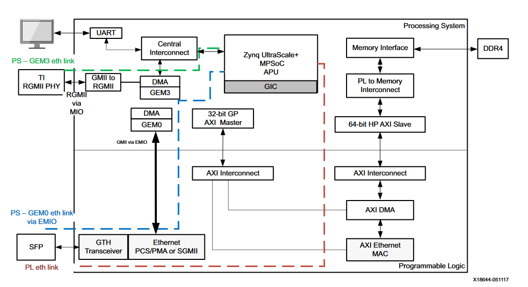
Figure 1: Zynq UltraScale+ MPSoC Ethernet Interface
Note: The PS-GEM3 is always tied to the TI RGMII PHY on the ZCU102 evaluation board. The 1000BASE-X/SGMII PHY and the GTH transceiver are a part of the AXI Ethernet core for 1G PL Ethernet link, which uses the AXI 1G/2.5G Ethernet subsystem IP core [Ref 1]. The PS-PL Ethernet uses PS-GEM0 and 1G/2.5G Ethernet PCS/PMA, or SGMII core [Ref 2]. The 10G PL Ethernet link uses 10/25G high-speed Ethernet subsystem IP core [Ref 3].
In the designs provided with this application note, the PS-GEM3 is connected to the Texas Instruments DP83867IRPAP Ethernet RGMII PHY device through the reduced gigabit media independent interface (RGMII). This is the default setup for the ZCU102 board. This application note demonstrates various PS and PL-based Ethernet implementations. The designs described in this application note are listed below.
PS Ethernet (GEM3) connected to a 1G physical interface in PS through an MIO interface. See Using PS GEM through MIO.
PS Ethernet (GEM0) connected to a 1000BASE-X/SGMII physical interface in PL through an EMIO interface. See Using PS GEM through EMIO.
Ethernet implemented as soft logic in PL (MAC) and connected to the 1000BASE-X/SGMII physical interface in PL. See Using PL 1G Ethernet.
Ethernet implemented as soft logic in PL (MAC) and connected to the 10G physical interface in PL. See Using PL 10G Ethernet.
Note: GEM0, GEM1, or GEM2 can also be used for PS Ethernet. The hardware design varies depending on the GEM selected.
Using PS GEM through MIO
This section describes how to use the PS Ethernet block GEM3 with the PS PHY through the MIO interface.
Hardware Design
The PS Ethernet controller (GEM3) connects the on-board TI PHY through MIO pins using the RGMII interface. The GEM3 block is enabled while generating the hardware system. The GEM3-TI PHY link is shown in Figure 1 with the PS-GEM3 link. For more information refer to the PS and PL based Ethernet in Zynq MPSoC wiki [Ref 4].
Reference Clock Generation
The Ethernet reference clock (125 MHz) for each of the GEMs is generated by configuring the internal PLL of the PS.
Software Design
This design uses the common macb.c driver code (present in the Linux kernel) for all the GEMs on the ZCU102. The macb driver uses the direct memory access (DMA) controller attached to the GEM in the PS. This driver is responsible for several functions including DMA descriptor rings setup, allocation, and recycling. The interrupt handling is done only for the PS GEM events because the interrupt status implicitly reflects DMA events. Additionally, the device tree is updated to include PS-GEM3 with relevant parameters. Refer to Device Trees for more information.
Linux Driver
A monolithic Linux device driver is used in this design. The software architecture for PS Ethernet interfaces is shown in Figure 2.
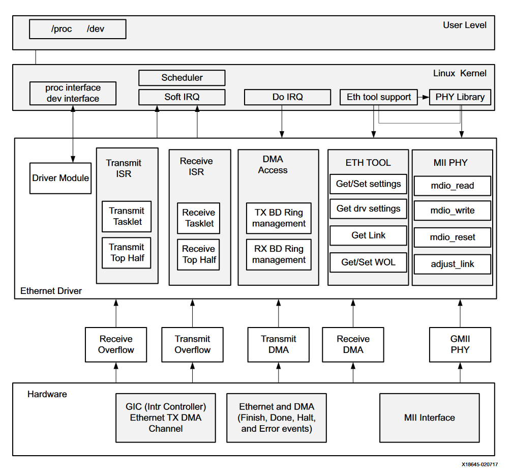
Figure 2: PS Ethernet Software Driver for Linux
Using PS GEM through EMIO
This section describes the use of the PS Ethernet block GEM0 with the PL PHY through the EMIO interface. The PS GEM block can be accessed through the PL using EMIO pins that allow GMII and management data input/output (MDIO) interfaces to be connected to the physical layer. The 1G/2.5G Ethernet PCS/PMA or SGMII core can be used as the physical media for the Ethernet in 1000BASE-X or SGMII mode. High-speed serial transceivers are used to access the small form factor pluggable (SFP) cage on the ZCU102 board. The SFP cage is connected to a standard Ethernet LAN through an SFP-to-RJ45 converter module. To enable the SFP, jumper J16 should be shorted as shown in Figure 7.
Hardware Design
As shown in Figure 3, the GMII interface connects the PHY and PS GEM through the EMIO pins. The GEM0 block is enabled while generating the hardware system in the Vivado® tools. The PHY address port of 1G/2.5G Ethernet PCS/PMA or serial gigabit media independent interface (SGMII) core can be assigned a fixed value in the range of 1 to 31. See the PS and PL based Ethernet in Zynq MPSoC wiki [Ref 4] and 1G/2.5G Ethernet PCS/PMA or SGMII v16.0 LogiCORE IP Product Guide (PG047) [Ref 2] for more information.
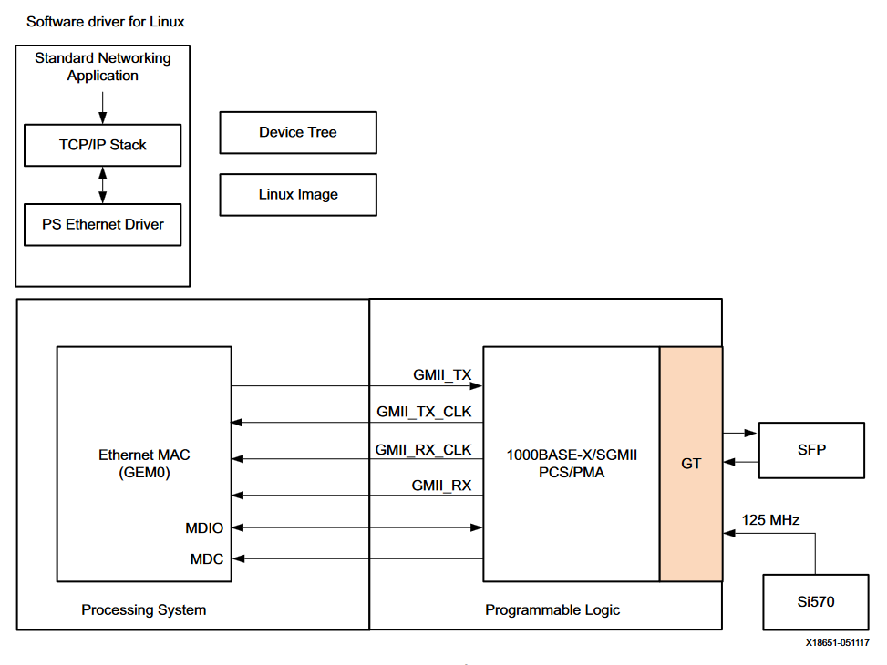
Figure 3: PS-PL Ethernet Design
Reference Clock Generation
The GTH transceivers X1Y12-X1Y15 on the Zynq UltraScale+ MPSoC are connected to the SFP cage on the ZCU102 board. The GTH transceiver reference clock (156.25 MHz differential) is generated from the Si570 jitter attenuator on the ZCU102 board. The clock divider values are adjusted to generate 156.25 MHz from the Si570 programmable oscillator. The Si570 is programmed over the I2C interface to generate the required clock value. See the Si570 data sheet [Ref 5] for details on the Si570.To enable GEM0 through the EMIO interface, specific registers must be programmed. This is part of the PS configuration data used by the Zynq UltraScale+ MPSoC first stage boot loader (FSBL). To select the EMIO as the source for receiving clock, data, and control signals, set the SLCR. GEM0_CLK_CTRL[SRCSEL] bit to 3'b1xx, where x is a don't care (1 or 0).
Software Design
This design uses the common macb.c driver code for all the GEMs on the ZCU102. The macb driver uses the DMA controller attached to the GEM in the PS. This driver is responsible for several functions, including DMA descriptor rings setup, allocation, and recycling. The interrupt handling is done only for the PS GEM events, because the interrupt status implicitly reflects DMA events. Additionally, the device tree is updated to include PS-GEM0 with relevant parameters. Refer to Device Trees for more information.
Note: To support other PL physical interfaces such as TBI, the hardware design and device tree must be edited. The PHY specific initialization is handled by the phylib subsystem in the Linux driver (macb), and information regarding the PHY can be provided in the device tree. To use the phylib subsystem for PHY programming, the phylib subsystem must support the PHY initialization routine for the desired PHY.
Linux Driver
A monolithic Linux device driver is provided for this design. Figure 2 shows the software architecture for the PS Ethernet interfaces
Using PL 1G Ethernet
This section describes the PL implementation of the Ethernet. This design consists of the AXI 1G/2.5G Ethernet subsystem, AXI DMA, and AXI Interconnect IP cores. The AXI 1G/2.5G Ethernet subsystem IP core consists of Tri-mode Ethernet MAC (TEMAC) and 1G/2.5G Ethernet PCS/PMA or serial gigabit media independent interface (SGMII) cores. A high performance (HP) port is used in this design for fast access to the PS-DDR memory. The general-purpose slave port can also be used if the HP port is occupied with other peripherals.
Hardware Design
Ethernet implementation in the PL is shown in Figure 4. The HP port is used for fast data transfers between the PL and the PS-DDR4 memory. It connects to the AXI DMA scatter-gather, stream to memory mapped (S2MM) and memory mapped to stream (MM2S) interfaces through the AXI interconnect. This interconnect also performs data width conversion to connect the 64-bit HP port to the 32-bit interfaces of the AXI DMA. In the AXI DMA, both the scatter-gather option and data realignment engine are enabled for the S2MM and MM2S paths. The streaming interface of the AXI DMA is connected to the AXI Ethernet subsystem. The AXI Ethernet subsystem has full checksum offloading (CSO) enabled and has FIFO depths of 32K to support jumbo frame transfers. The AXI Ethernet core implements an Ethernet MAC and supports 1000BASE-X and SGMII PHY interfaces. It connects to the SFP through GTH transceivers through 1000BASE-X/SGMII interfaces. For the control interface, a general purpose (GP) AXI master port is enabled in the PS. This port connects to the AXI DMA and AXI Ethernet cores.The 1000BASE-X and SGMII PHY registers are accessed using the MDIO interface provided by the AXI Ethernet core. The interrupt ports from the AXI DMA and the AXI Ethernet IP cores are connected to the general interrupt controller (GIC) in the PS. For more information refer to the PS and PL based Ethernet in Zynq MPSoC wiki [Ref 4]. For further details on IP cores, see the AXI 1G/2.5G Ethernet Subsystem v7.0 Product Guide(PG138) [Ref 1], 1G/2.5G Ethernet PCS/PMA or SGMII v16.0 LogiCORE IP Product Guide (PG047) [Ref 2], and AXI DMA v7.1 LogiCORE IP Product Guide (PG021) [Ref 6].
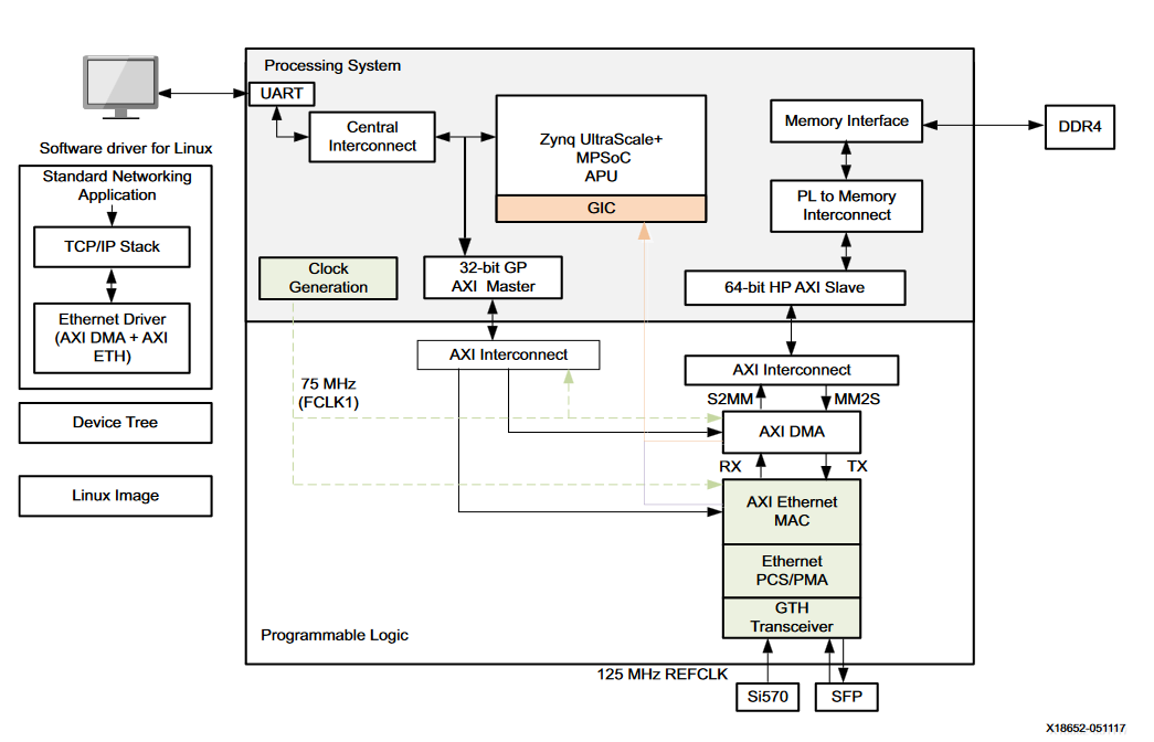
Figure 4: 1000BASE-X/SGMII PL Ethernet Design
Reference Clock Generation
The GTH transceivers X1Y12-X1Y15 on the Zynq UltraScale+ MPSoC are connected to the SFP cage on the ZCU102 board for 1000BASE-X/SGMII transceivers. The GTH transceiver reference clock (156.25 MHz differential) is generated from the Si570 jitter attenuator on the ZCU102 board. The clock divider values are adjusted to generate 156.25 MHz from the Si570 programmable oscillator. The Si570 is programmed over the I2C interface to generate the required clock value. See the Si570 data sheet [Ref 5] for details on the Si570.
Software Design
This section describes the software aspects of the design. The monolithic Linux driver code facilitates the functionality listed below.
PL Ethernet MAC accesses
AXI DMA transfers
Physical media initialization for 1000BASE-X interface using the phylib subsystem
Linux Driver
The software architecture for this design is shown in Figure 5. The driver is divided into the following sections.
Initialization
MAC driver hooks
Interrupt service routines

Figure 5: Driver Architecture for PL Ethernet
Using PL 10G Ethernet
This section describes a PL implementation of the 10G Ethernet. The design consists of 10G/25G high-speed Ethernet subsystem, AXI DMA, and AXI Interconnect IP cores. This design uses the high performance (HP) port for fast access to the PS-DDR memory. The general purpose slave port can also be used if the HP port is occupied with other peripherals.
Hardware Design
The 10G Ethernet implementation in PL is shown in Figure 6. The Xilinx 10G/25G high speed Ethernet subsystem implements the 25G Ethernet MAC with a physical coding sublayer (PCS) as specified by the 25G Ethernet Consortium. The 156.25 MHz reference clock to the transceiver is provided by the Si570 programmable oscillator available on the ZCU102 board. For more information refer to the PS and PL based Ethernet in Zynq MPSoC wiki [Ref 4].
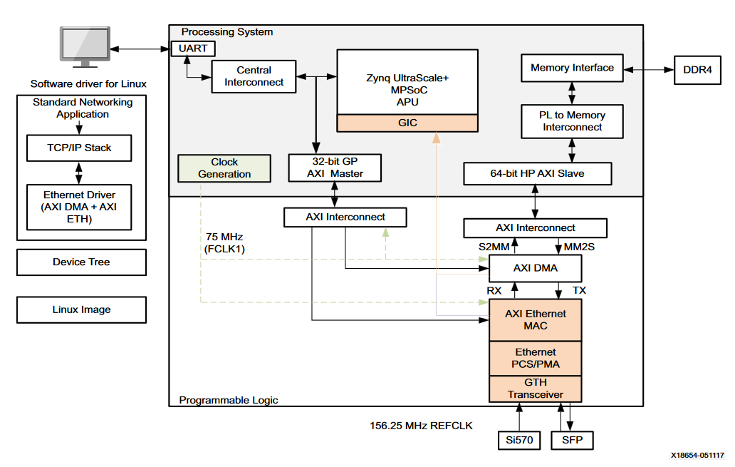
Figure 6: 10G PL Ethernet Design
Reference Clock Generation
The GTH transceivers X1Y12-X1Y15 on the Zynq UltraScale+ MPSoC are connected to the SFP cage on the ZCU102 board. The GTH transceiver reference clock (156.25 MHz differential) is generated from the Si570 jitter attenuator on the ZCU102 board. The clock divider values are adjusted to generate 156.25 MHz from the Si570 programmable oscillator. The Si570 is programmed over the I2C interface to generate the required clock value. See the Si570 data sheet [Ref 5] for details on the Si570.
Software Design
This section describes the software aspects of the design. The monolithic Linux driver code facilitates the functionality listed below.
PL Ethernet MAC accesses
AXI DMA transfers
Linux Driver
The software architecture for this design is shown in Figure 5. The driver is divided into the following sections.
Initialization
MAC driver hooks
Interrupt service routines
References
AXI 1G/2.5G Ethernet Subsystem v7.0 Product Guide (PG138)
1G/2.5G Ethernet PCS/PMA or SGMII v16.0 LogiCORE IP Product Guide (PG047)
10G/25G High Speed Ethernet Subsystem v2.0 Product Guide (PG210)
PS and PL based Ethernet in Zynq MPSoC
Si570 Data Sheet (www.silabs.com/Support%20Documents/TechnicalDocs/Si570.pdf)
AXI DMA v7.1 LogiCORE IP Product Guide (PG021)
Netperf(www.netperf.org)
Xilinx Vivado Design Suite
PetaLinux
Zynq UltraScale+ MPSoC Technical Reference Manual (UG1085)
ZCU102 Evaluation Board User Guide (UG1182)13.UltraScale Architecture GTH Transceivers User Guide (UG576)