In the 2018.2 version of the design, all the features were part of a single monolithic design. In the current version (2018.3), subsequent version the design has been split into three example designs based on the functionality (MTS only design, Non MTS design and SSR IP design). This section describes 8x8 (8-DAC, 8-ADC) channel Non-MTS design. This example design demonstrates most of the features of RFDC IP except for Multi-Tile Sync (MTS).
The data path for Non-MTS design remains almost similar to that of the 2018.2 version of monolithic design except for the reduced buffer sizes and simplification of clocking structure.
The contents of this page are as mentioned below.
| Table of Contents |
|---|
New Feature Addition
In 2018.2 version of design the data was captured sequentially for all the ADC based on the GUI request that itself came sequentially. In the current subsequent version (2018.3) data is simultaneously captured for all the 8-ADC channels and provided to GUI sequentially. This now enables the user to simultaneously capture very large sample sizes by making use of large DDR storage.The performance numbers related to DAC/ADC is published on Performance Tables Appendix A Performance Table (of the ZCU111 RFSoC RF Data Converter Evaluation Tool Getting Started Guide).
Clock and Control Changes
The design is clocked with the respective DAC and ADC clocks. There is no usage of PL Clock/SysRef clock in non MTS Mode. Hence the Clock Muxes (BUFGMUXs) have been removed from the design. The channels are clocked using clocks derived from their respective tiles and not from a common source as is the case in MTS design. This design has individual channel start/trigger signals and the common channel start/trigger signal required for MTS is removed. Hence the corresponding GPIO is also removed. The updated design constraint file is updated as a part of the Non-MTS design example design package.
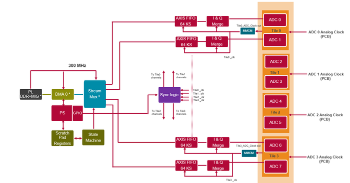
The following is the block diagram of the Non MTS design (DAC side),Corresponding changes are there on ADC side also.
For DAC
...